High-conversion rate silicon crystal and thin film compound type unijunction PIN (Positive Intrinsic-Negative) solar battery and manufacturing method thereof

A solar cell, high conversion rate technology, applied in the field of solar cells

Active Publication Date: 2010-11-24
湖南共创光伏科技有限公司
View PDF1 Cites 11 Cited by
  • Summary
  • Abstract
  • Description
  • Claims
  • Application Information

AI Technical Summary

Problems solved by technology

[0017] The technical problem to be solved by the present invention is to propose a high-conversion silicon crystal and thin film composite solar cell by combining monocrystalline silicon and polycrystalline silicon-based single-unit solar cells with silicon-based thin-film solar cells, aiming at the deficiencies in the prior art. Type single-junction PIN solar cell and manufacturing method thereof, described high-conversion rate silicon crystal and thin-film composite single-junction PIN solar cell have higher conversion efficiency and excellent stability

Method used


Image

  • High-conversion rate silicon crystal and thin film compound type unijunction PIN (Positive Intrinsic-Negative) solar battery and manufacturing method thereof
  • High-conversion rate silicon crystal and thin film compound type unijunction PIN (Positive Intrinsic-Negative) solar battery and manufacturing method thereof
  • High-conversion rate silicon crystal and thin film compound type unijunction PIN (Positive Intrinsic-Negative) solar battery and manufacturing method thereof

Examples


Embodiment 1

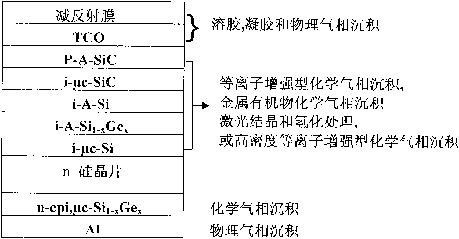
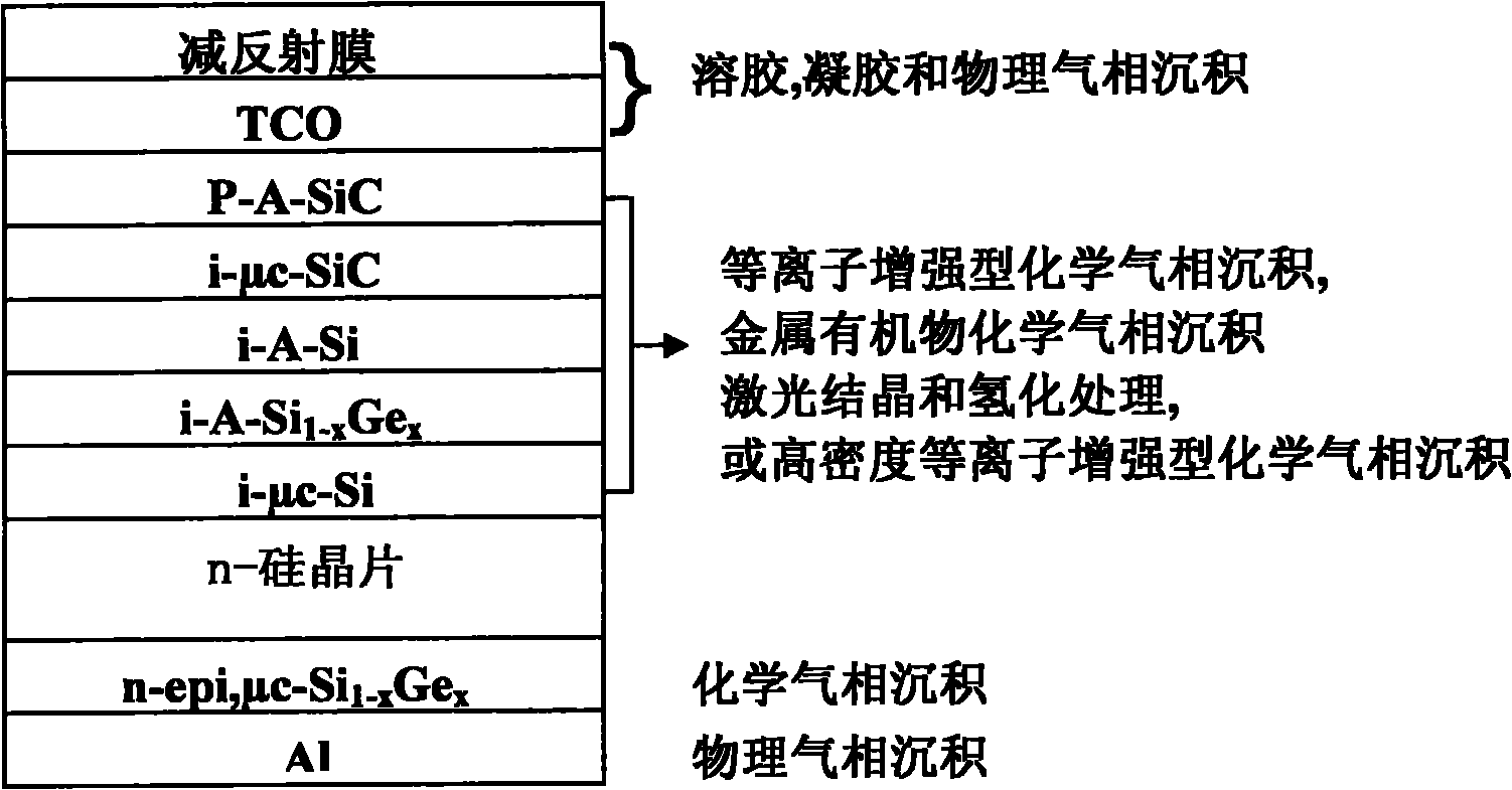
[0060] Example 1: A silicon crystal and thin film compound single-junction PIN solar cell single-junction six-layer pin structure thin-film solar cell, the structure is:

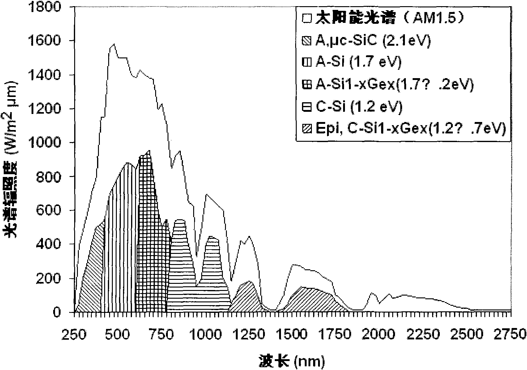
[0061] Bottom electrode / n-type gradient μc or epi Si 1-x Ge x / n-type silicon wafer / i-μc-Si / i-A-Si 1-x Ge x / i-A-Si / i-μc-SiC / p-A-SiC / TCO / anti-reflection coating.

Embodiment 2

[0062] Embodiment 2: preparation method

[0063] a. High-conversion silicon crystal and thin-film composite single-junction PIN solar cells Single-junction six-layer pin structure thin-film solar cells, the structure is: bottom electrode / n-type gradient g μc or epi Si 1-x Ge x / n-type silicon wafer / i-μc-Si / i-A-Si 1-x Ge x / i-A-Si / i-μc-SiC / p-A-SiC / TCO / anti-reflection coating.

[0064] b. Preparation process:

[0065] 1. Chemical and mechanical (CMP) double-sided polishing of n-type silicon wafers (monocrystalline or polycrystalline); then,

[0066] 2. Cleaning of n-type silicon wafers (single crystal silicon wafers or polycrystalline silicon wafers);

[0067] 3. Use PECVD to form silicon-rich silicon oxide or TCO intermediate reflection layer film;

[0068] 4. On the front side of n-type silicon wafers (single crystal silicon wafers and polycrystalline silicon wafers), deposit phosphorus (P) doped n-type Ge by CVD method, and n-type gradient μc or epi Si 1-x Ge x Thin f...


PUM

PropertyMeasurementUnit
Apertureaaaaaaaaaa
Membrane thicknessaaaaaaaaaa

Abstract

The invention provides a high-conversion rate silicon crystal and thin film compound type unijunction PIN (Positive Intrinsic-Negative) solar battery and a manufacturing method thereof. The battery is in the structure of a bottom electrode / n-shaped gradient mu c or epi Si1-xGex / n-shaped silicon chip / i-mu-Si / i-A-si1-xGex / i-A-Si / i-mu c-SiC / p-A-SiC / TCO / a reflection reduction film. In the single-crystal multi-i layer PIN structure, the i layers can be selected from the six materials to form a two-layer, three-layer, four-layer, five-layer and six-layer structure; the interface performance among the layers is improved by adopting a laser crystallization process, a plasma doping process and a CVD (Chemical Vapor Deposition) and PECVD (Plasma Enhanced Chemical Vapor Deposition) transition layer process, and the performance stability of each-layer material is kept and the light transmittance and the electrical conductivity of a transparent conductive thin-film material and an interface are improved by using a hydrotreating process; and the conversion efficiency of the battery is expected to reach 25%-30%, and the battery has better stability.

Description

technical field [0001] The invention relates to a solar cell, in particular to a silicon crystal and silicon-based thin film solar cell structure and a manufacturing method thereof. Background technique [0002] Since the French scientist AE. Becquerel discovered the photoelectric conversion phenomenon in 1839, the first solar cell based on semiconductor selenium was born in 1883. RuSSell obtained the first solar cell patent (US.2,402,662) in 1946, and its photoelectric conversion efficiency was only 1%. It was not until 1954 that Bell Laboratories' research discovered that doped silicon-based materials have high photoelectric conversion efficiency. This research laid the foundation for the modern solar cell industry. In 1958, the Haffman Power Company of the United States installed the first solar panel on a satellite in the United States, and its photoelectric conversion efficiency was about 6%. Since then, the research and production of solar cells on monocrystalline s...

Claims


Application Information

Patent Timeline
IPC IPC(8): H01L31/042H01L31/06H01L31/18H01L31/20H01L31/077
CPCY02E10/52Y02E10/547Y02E10/548Y02P70/50
Inventor 李廷凯李晴风钟真陈建国
Owner 湖南共创光伏科技有限公司
Why Eureka
Try Eureka