Gain cell eDRAM for programmable logic device

A technology for programming logic and devices, applied in the field of embedded dynamic random access memory, can solve the problems of low destructive readout degree, weak turn-on and turn-off degree, destructive read operation, etc., and achieve the effect of reducing the chip area

Inactive Publication Date: 2010-12-08
FUDAN UNIV
View PDF2 Cites 6 Cited by
  • Summary
  • Abstract
  • Description
  • Claims
  • Application Information

AI Technical Summary

Problems solved by technology

[0006] However, the above figure 1 and figure 2 When the DRAM storage unit of the illustrated embodiment is applied to a programmable logic device, its main disadvantage is that the read operation is destructive, and the refresh operation is read first and then written, and the parasitic capacitance passes through the MOS gate during the read operation. Charge and discharge the parasitic capacitance (the read operation during the refresh operation is also destructive), at this time, due to the potential change of the parasitic capacitance, the state of the switch tube will change (conduction to off, or off to on, or conduction The degree of on-off becomes weaker), this change in the state of the switch will cause the logic state of the programmable logic device to be wrong
[0013] It

Method used


Image

  • Gain cell eDRAM for programmable logic device
  • Gain cell eDRAM for programmable logic device
  • Gain cell eDRAM for programmable logic device

Examples


Embodiment Construction

[0024] In order to make the object, technical solution and advantages of the present invention clearer, the present invention will be further described in detail below in conjunction with the accompanying drawings.

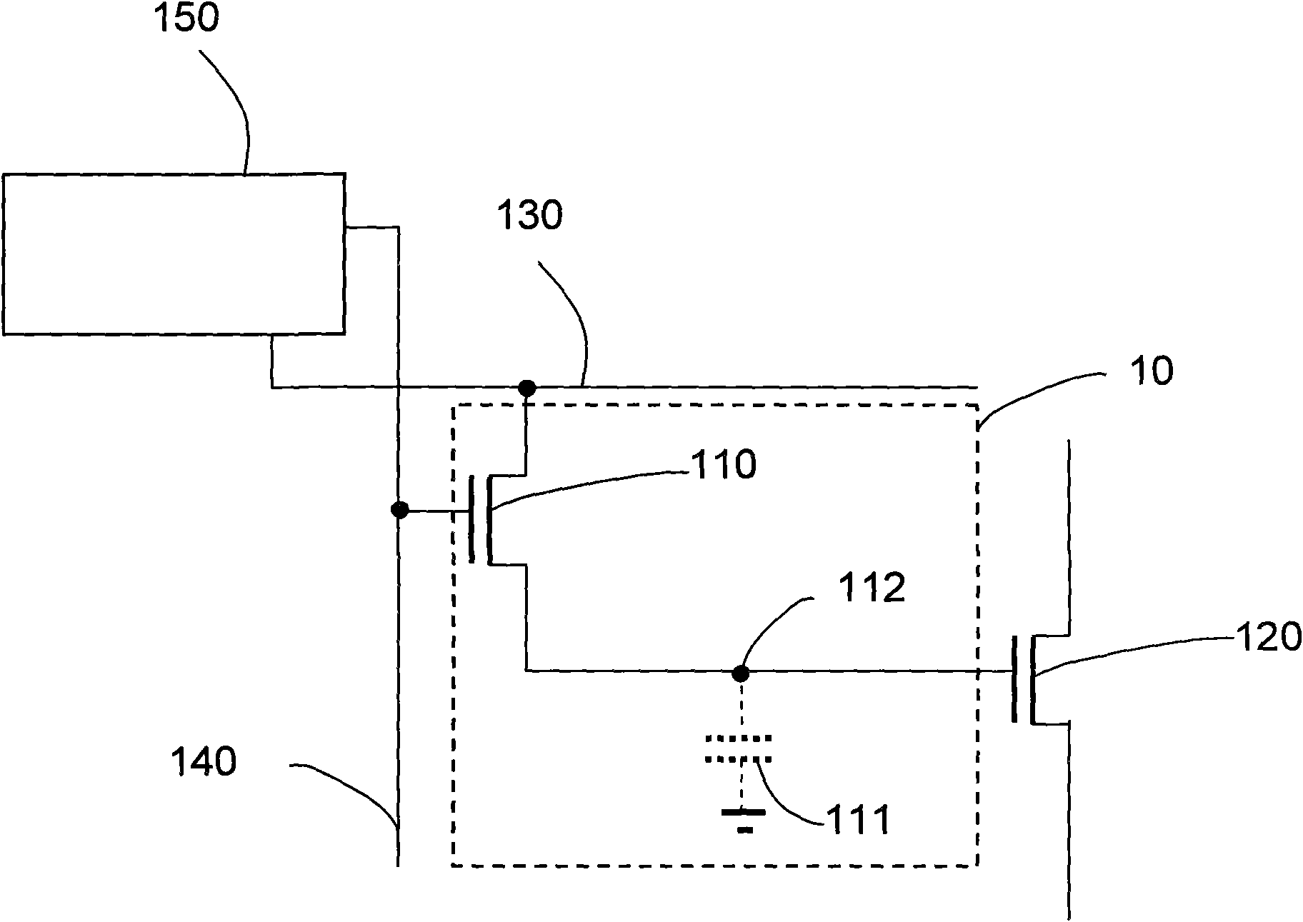
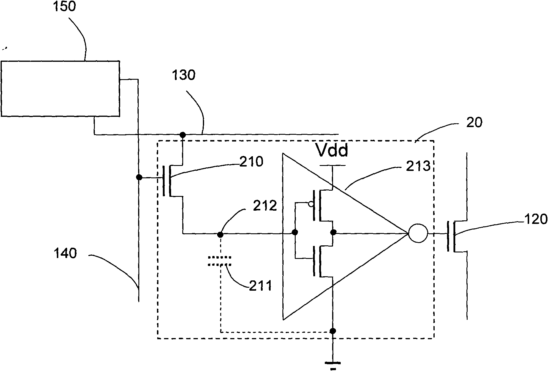
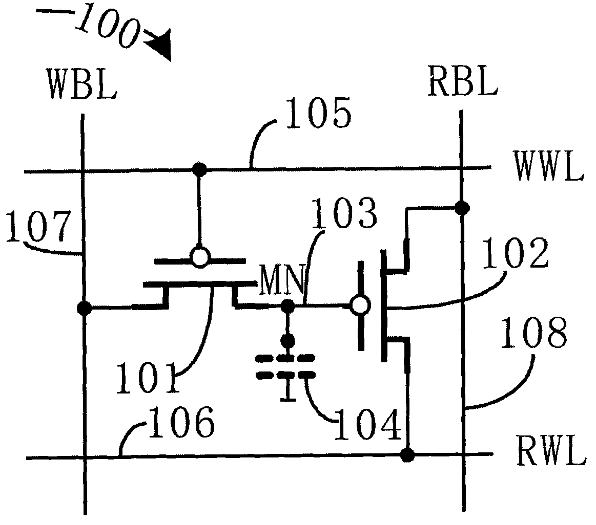
[0025] Figure 4 Shown is a schematic structural diagram of a gain unit eDRAM according to an embodiment of the present invention. In this embodiment, the gain unit eDRAM 300 is used for the configuration memory of the programmable logic device, and is used to control the on and off of the switching tube. The switching tube is one of the basic units of the programmable logic device, and its logic state reflects the programmable The programming state of the logic device. In this invention, the programmable logic device not only refers to PLD, but also includes FPGA and other programmable logic devices with basically the same principle. Such as Figure 4 As shown, the gain unit eDRAM 300 includes a write MOS transistor 301, a read MOS transistor 302, a write word...


PUM


Abstract

The invention belongs to the technical field of embedded dynamic random access memories (eDRAM), and in particular relates to a gain cell eDRAM for a programmable logic device. The gain cell eDRAM in the invention comprises a read MOS transistor, a write MOS transistor, a write word line, a read word line, a write bit line, a read bit line and an equivalent parasitic capacitor, wherein a charge storage end of the equivalent parasitic capacitor controls a switch tube of the programmable logic device; and by using the characteristic of non-destructive read or small destructive read of the gain cell eDRAM, the potential of a storage node does not change or the potential change is small when read operation is performed during updating operation, so the change of the logic state of the switch tube is not influenced. The chip area of the programmable logic device using the gain cell eDRAM can be greatly reduced.

Description

technical field [0001] The invention belongs to the technical field of embedded dynamic random access memory (eDRM), and in particular relates to a gain cell (Gain Cell) eDRAM used for a programmable logic device. Background technique [0002] PLD is the abbreviation of Programmable Logic Device, and FPGA is the abbreviation of Field Programmable Gate Array (Field Programmable GateArray). Ignoring the difference between the two, PLD and FPGA are collectively referred to as programmable logic devices. Programmable logic devices can complete the functions of any digital device, ranging from high-performance CPUs to simple 74 circuits, all of which can be implemented with PLDs. Programmable logic devices are like a piece of white paper or a pile of building blocks. Engineers can freely design a digital system through traditional schematic diagram input methods or hardware description languages. Through software simulation, the correctness of the design can be verified in adva...

Claims


Application Information

Patent Timeline
IPC IPC(8): G11C11/405G11C11/409
Inventor 林殷茵薛晓勇
Owner FUDAN UNIV
Why Eureka
Try Eureka