Method for preparing large-area polycrystalline film

A large-area, amorphous silicon thin-film technology, used in final product manufacturing, sustainable manufacturing/processing, semiconductor/solid-state device manufacturing, etc. Improved photoelectric conversion efficiency, shortened process time, and high electron mobility

Inactive Publication Date: 2010-12-08
江苏华创光电科技有限公司
View PDF2 Cites 11 Cited by
  • Summary
  • Abstract
  • Description
  • Claims
  • Application Information

AI Technical Summary

Problems solved by technology

Polysilicon thin films prepared by laser-induced crystallization have the characteristics of high mobility and good space selectivity, but poor repeatability, stability, and uniformity, making it difficult to large-scale, while metal induction can effectively solve the shortcomings of laser induction, but Metal induction also has the characteristics that the crystallization rate is not high enough, the heat treatment time is long, and the crystallization rate decreases with the increase of heat treatment time. The polysilicon thin film manufactured by the technology has the following characteristics, it can be prepared in a large area, has a preferred orientation, high electron mobility, and is easy to industrialize in a short time. The traditional low-temperature method of manufacturing polysilicon is us

Method used


Image

  • Method for preparing large-area polycrystalline film
  • Method for preparing large-area polycrystalline film

Examples


Embodiment 1

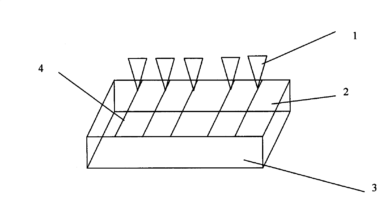
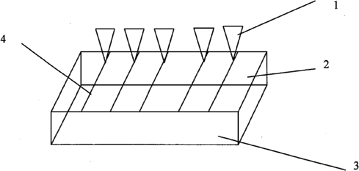
[0026] Combine below figure 1 The present invention is described further, and concrete process is as follows:

[0027] 1. Prepare a piece of ultra-clear glass 3. It is required to have better light transmittance. Deposit a-Si:H thin film 2 with PECVD method, thickness is for 150nm, with SiH 4 and H 2 As the reaction gas, the gas flow rate is 18mL / min, the substrate temperature is 220°C, and the reaction chamber pressure is 80Pa.

[0028] 2. On the basis of step 1, the strip window 4 is exposed by using a photolithography process, and the distance between the two strip windows is determined according to actual needs, and the distance is at the millimeter level.

[0029] 3. On the basis of step 2, use the magnetron sputtering method to sputter a layer of Ni metal layer on the amorphous silicon film, the position is on the amorphous silicon layer at the opened window, the thickness is 10nm, and the radio frequency sputtering power density 4W / cm 2 The substrate temperature is...


PUM

PropertyMeasurementUnit
Thicknessaaaaaaaaaa

Abstract

The invention discloses a method for preparing a large-area polycrystalline film, which comprises the following steps of: (1) depositing a layer of amorphous silicon film on a glass substrate; (2) exposing a strip window on the amorphous silicon film by adopting a photo-etching process; (3) sputtering a layer of metal on the amorphous silicon film in the window by adopting a magnetron sputtering method; (4) irradiating the window by adopting a laser device to prepare the polycrystalline film; and (5) removing the residual nickel metal by using acid. The invention provides the new method for preparing the polycrystalline film by combining a conventional metal-induced solid phase crystallization method and a laser crystallization technique; the prepared polycrystalline film has the effects on preferred orientation of the metal-induced solid phase crystallization method and high mobility and few defects of the laser crystallization method; and meanwhile, the method can prepare the large-area polycrystalline film by combining the photo-etching technology and the metal-induced transverse crystallization property, and provides convenience for industrialization.

Description

technical field [0001] The invention relates to a novel method for manufacturing a metal-induced polysilicon film, in particular to a method for preparing a polysilicon film with preferred orientation and high mobility. Background technique [0002] The light attenuation characteristics and conversion efficiency of amorphous silicon thin film solar cells are not high, so people turn more attention to polycrystalline silicon thin films. Using polycrystalline instead of amorphous can solve the problem of light attenuation, and the conversion efficiency will decrease due to the reduction of defects. It has been further improved. At present, there are two main methods for preparing low-temperature crystallized amorphous silicon: laser-induced crystallization (ELA) and metal-induced crystallization (MIC / MILC). Polysilicon thin films prepared by laser-induced crystallization have the characteristics of high mobility and good space selectivity, but poor repeatability, stability, an...

Claims


Application Information

Patent Timeline
IPC IPC(8): H01L21/20H01L31/18
CPCY02P70/50
Inventor 张宏勇邹福松
Owner 江苏华创光电科技有限公司
Why Eureka
Try Eureka