

Method for preparing gate stack of metallic nano crystal memory
A metal nanocrystal and memory technology, which is applied in semiconductor/solid-state device manufacturing, semiconductor devices, electrical components, etc., can solve the problems of poor metal nanocrystal uniformity, high annealing temperature, and complicated process, so as to avoid application bottlenecks and high cost effect
- Summary
- Abstract
- Description
- Claims
- Application Information
AI Technical Summary
Problems solved by technology
Method used
Image

Examples
Embodiment Construction
[0029] Below in conjunction with accompanying drawing, the present invention is described in detail.
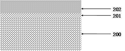
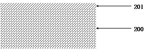
[0030] Step 1: Refer to figure 1 , deposit a layer 201 on the substrate 200 as a charge tunneling layer, wherein 200 is a single crystal silicon wafer; 201 is an atomic layer deposited Al 2 o 3 The thin film has a thickness of 5-12 nanometers.
[0031] Step 2: Refer to figure 2 , spin coating a layer of 202 on the 201, wherein 202 is a polyimide film with a thickness of 30-100 nanometers.
[0032] Step 3: Reference image 3 , place 203 on 202 and make them in close contact, wherein 203 is an alumina template, and the aperture of the template is 20-30 nanometers.
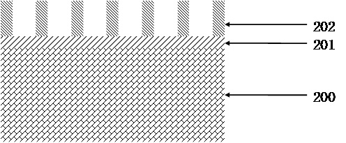
[0033] Step 4: Reference Figure 4 , using 203 as a mask to carry out reactive ion etching on 202, and the etching atmosphere is oxygen plasma.
[0034] Step 5: Reference Figure 5 , remove 203 by mechanical stripping or acid etching.
[0035] Step 6: Reference Figure 6 A layer of metal 204 is deposited ...
PUM
| Property | Measurement | Unit |
|---|---|---|
| thickness | aaaaa | aaaaa |
| thickness | aaaaa | aaaaa |
Abstract
Description
Claims
Application Information