Three-dimensional micro-heater comprising circular arc-shaped heating film region with adjustable radian and method
A technology of heating film area and heater, applied in the field of three-dimensional micro heater
- Summary
- Abstract
- Description
- Claims
- Application Information
AI Technical Summary
Problems solved by technology
Method used
Image
Examples
Embodiment 1
[0044] The structure diagram of this embodiment can be found in Figure 5 As shown, the specific production method is as follows:
[0045] 1. Selection of silicon substrate: choose a 4-inch silicon wafer with an N-type (110) surface as the substrate, with a resistivity of 1-10Ω·cm, and a silicon wafer thickness of 450±10 microns.
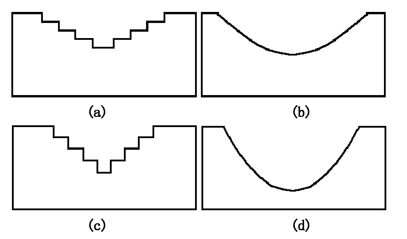
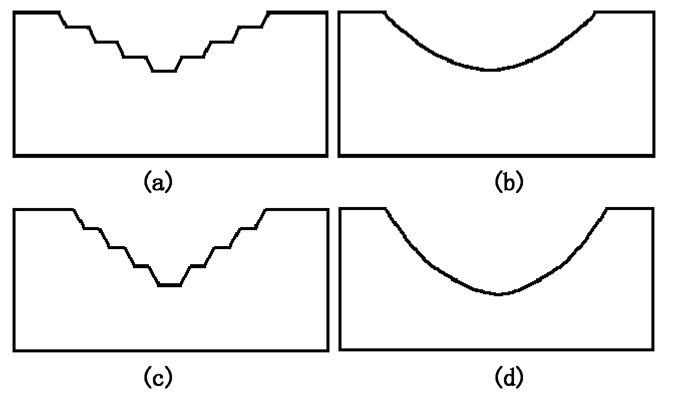
[0046] 2. Making stepped grooves: use silicon oxide as a mask, and form grooves with a series of steps through multiple times of silicon anisotropic dry etching. Silicon anisotropic dry etching can use DRIE (DeepReactive Ion Etching).
[0047] 3. Make a groove with a circular arc-shaped cross section: under the protection of silicon oxide, use the method of silicon isotropic dry etching to etch the stepped groove formed in step 2. At this time, the gas will Perform chamfer etching. The final groove depth is about 50 microns.
[0048] 4. Multiple oxidations to make the interior of the arc-shaped groove smoother: oxidize the silicon wafer after dr...
Embodiment 2
[0054] The structure diagram of this embodiment can be found in Figure 7 As shown, the specific production method is as follows:
[0055] 1. Selection of silicon substrate: select a 4-inch silicon wafer with a P-type (111) plane as the substrate, with a resistivity of 1-10Ω·cm, and a silicon wafer thickness of 450±10 microns.
[0056] 2. Making stepped grooves: use silicon oxide as a mask, and form grooves with a series of steps through multiple times of silicon anisotropic dry etching. Silicon anisotropic dry etching can use DRIE (DeepReactive Ion Etching).
[0057] 3. Make a groove with a circular arc-shaped cross section: under the protection of silicon oxide, use the method of silicon isotropic dry etching to etch the stepped groove formed in step 2. At this time, the gas will Perform chamfer etching. The final groove depth is about 50 microns.
[0058] 4. Multiple oxidations to make the interior of the arc-shaped groove smoother: oxidize the silicon wafer after dry e...
Embodiment 3
[0064] The structure diagram of this embodiment can be found in Figure 8 As shown, the specific production method is as follows:
[0065] 1. Selection of silicon substrate: choose a 4-inch silicon wafer with an N-type (100) plane as the substrate, with a resistivity of 3-8Ω·cm, and a silicon wafer thickness of 350±10 microns.
[0066] 2. Making stepped grooves: use silicon oxide as a mask, and form grooves with a series of steps by multiple times of silicon anisotropic wet etching. There are many options for silicon anisotropic etchant, such as: KOH (potassium hydroxide), TMAH (tetramethylammonium hydroxide), or EPW (ethylenediamine, catechol and water).
[0067] 3. Make a groove with a circular arc-shaped cross section: under the protection of silicon oxide, use the method of silicon isotropic dry etching to etch the stepped groove formed in step 2. At this time, the gas will Perform chamfer etching. The final groove depth is about 40 microns.
[0068] 4. Multiple oxidat...
PUM
| Property | Measurement | Unit |
|---|---|---|
| Thickness | aaaaa | aaaaa |
| Resistivity | aaaaa | aaaaa |
| Thickness | aaaaa | aaaaa |
Abstract
Description
Claims
Application Information


