
Three-dimensional micro heater with groove-shaped heating film region and manufacturing method thereof
A technology of heating film area and heater, applied in the field of micro-electro-mechanical systems, to achieve the effects of low cost, reduced heat loss, and simple process
- Summary
- Abstract
- Description
- Claims
- Application Information
AI Technical Summary
Problems solved by technology
Method used
Image

Examples
Embodiment 1
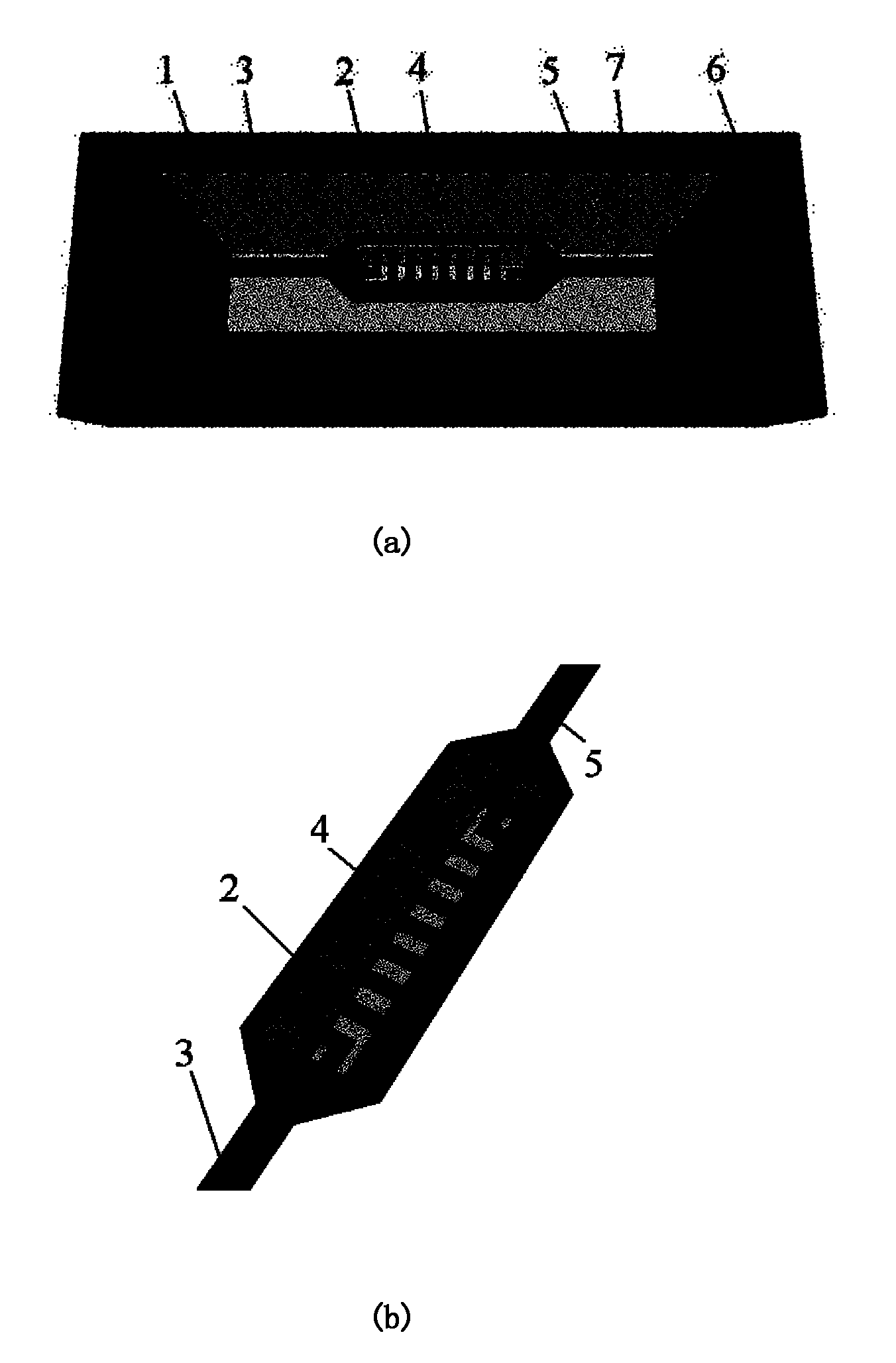
[0036] The structure diagram of this embodiment can be found in figure 1 As shown in (a), the specific production method is as follows:
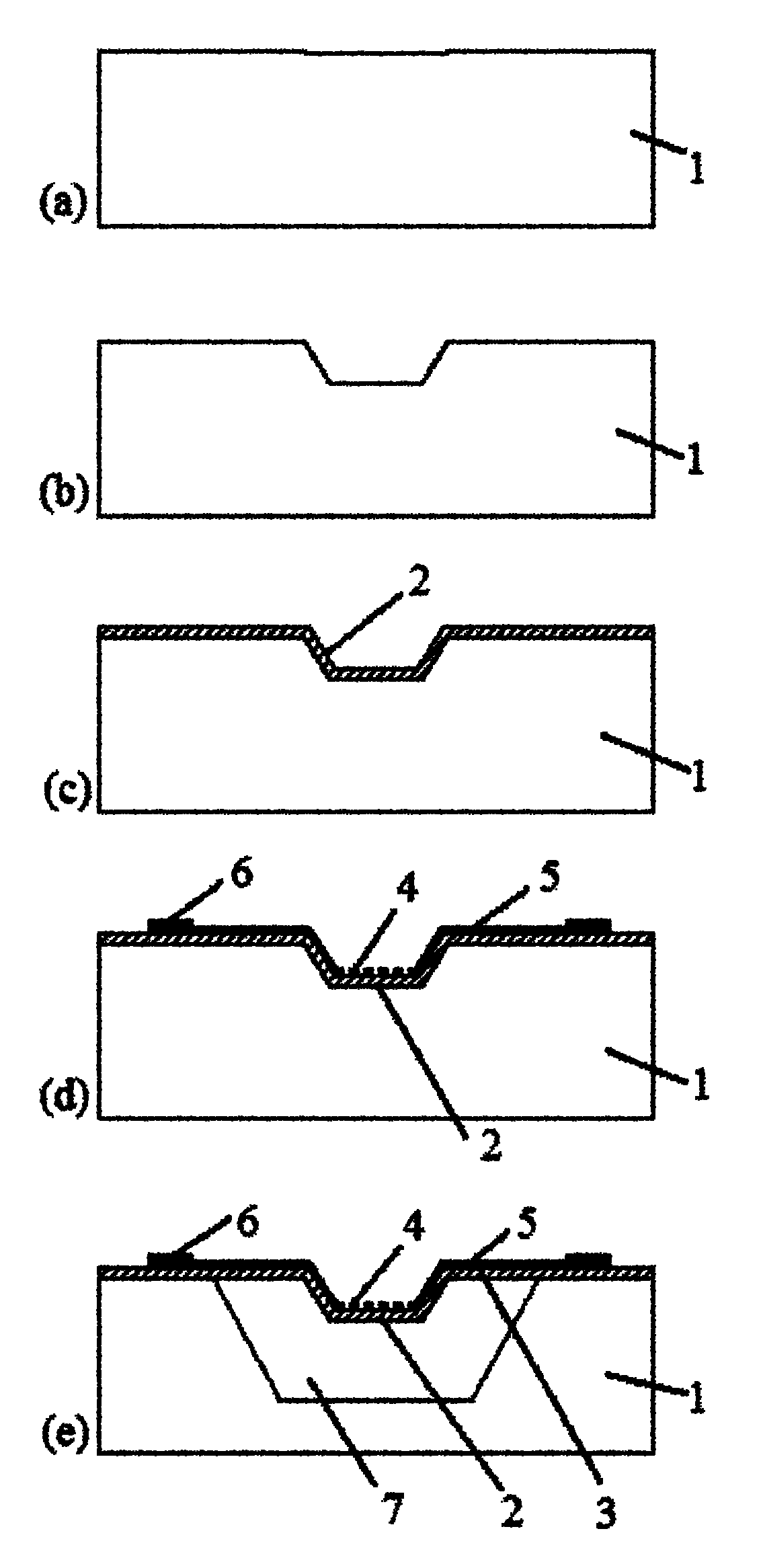
[0037] 1. Substrate selection. A 4-inch silicon wafer with an N-type (100) plane is selected as the substrate, the resistivity is 3-8Ω·cm, the thickness of the silicon wafer is 350±10 microns, and the angle error of trimming is less than 1%.
[0038] 2. Fabrication of front-side etched windows for formation of recessed structures. First, a silicon oxide film with a thickness of 1.0 microns is grown on the surface of the silicon wafer by thermal oxidation. Then perform front photolithography to make a window pattern, and use reactive ion etching (RIE) to completely etch the exposed silicon oxide under the protection of the photoresist to form a front etching window.
[0039] 3. Make a groove with a "V" shape or an inverted trapezoidal structure in cross section. Under the protection of silicon oxide, use KOH etching solution to etch out ...
Embodiment 2
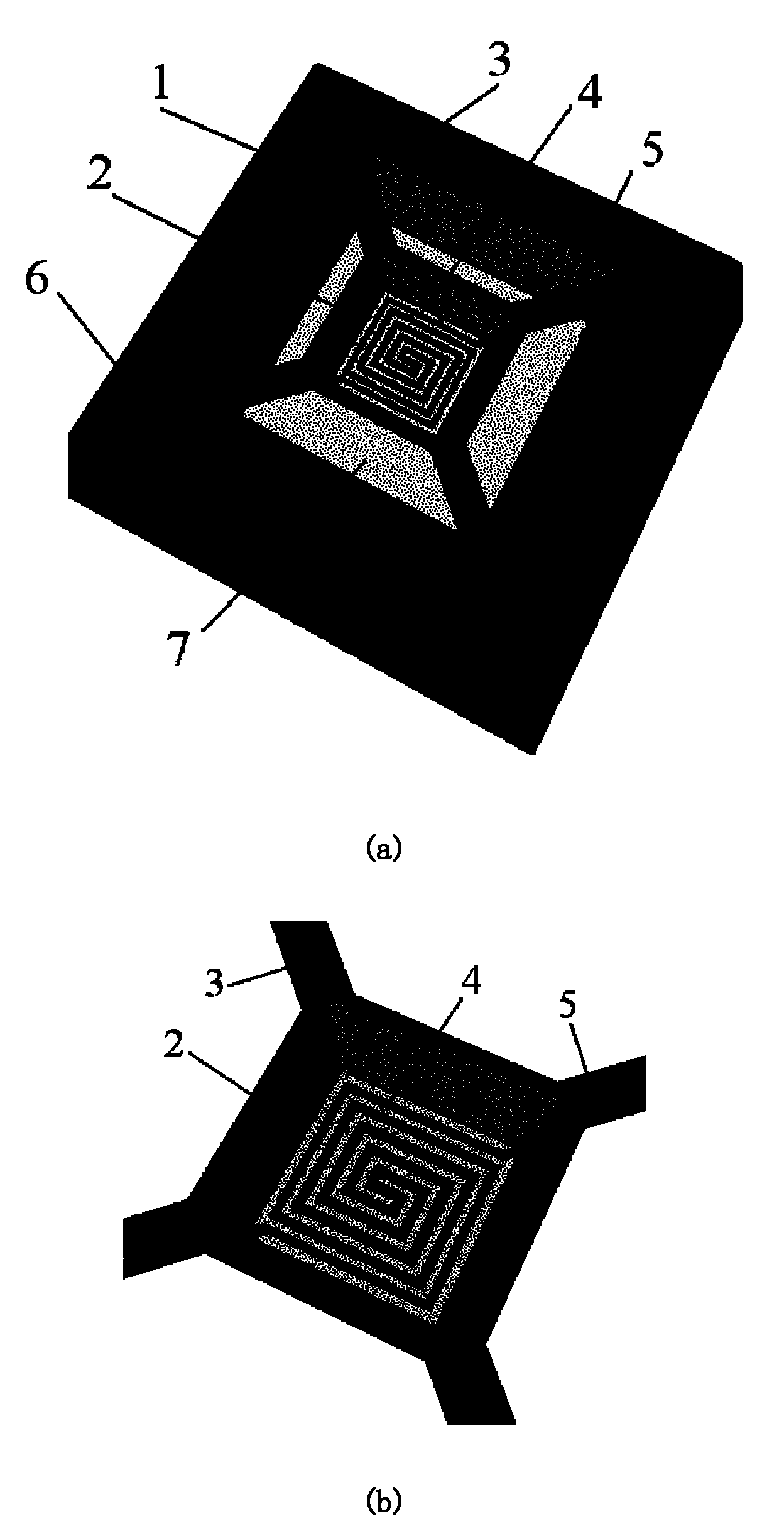
[0046] The structure diagram of this embodiment can be found in figure 2 As shown in (a), the specific production method is as follows:
[0047] 1. Substrate selection. A 4-inch silicon wafer with an N-type (100) plane is selected as the substrate, the resistivity is 3-8Ω·cm, the thickness of the silicon wafer is 350±10 microns, and the angle error of trimming is less than 1%.
[0048] 2. Fabrication of front-side etched windows for formation of recessed structures. First, a silicon oxide film with a thickness of 1.0 microns is grown on the surface of the silicon wafer by thermal oxidation. Then perform front photolithography to make a window pattern, and use reactive ion etching (RIE) to completely etch the exposed silicon oxide under the protection of the photoresist to form a front etching window.
[0049] 3. Make a groove with a "V" shape or an inverted trapezoidal structure in cross section. Under the protection of silicon oxide, use KOH etching solution to etch out ...
Embodiment 3
[0056] The structure diagram of this embodiment can be found in Figure 4 As shown, the specific production method is as follows:
[0057] 1. Substrate selection. A 4-inch silicon wafer with an N-type (100) plane is selected as the substrate, the resistivity is 3-8Ω·cm, the thickness of the silicon wafer is 450±10 microns, and the angle error of trimming is less than 1%.
[0058] 2. Fabrication of front-side etched windows for formation of recessed structures. First, a silicon oxide film with a thickness of 1.5 microns is grown on the surface of a silicon wafer by means of low-pressure chemical vapor deposition (LPCVD). Then perform front photolithography to make a window pattern, and use reactive ion etching (RIE) to completely etch the exposed silicon oxide under the protection of the photoresist to form a front etching window.
[0059] 3. Make a groove with a "V" shape or an inverted trapezoidal structure in cross section. Under the protection of silicon oxide, use KOH ...
PUM
| Property | Measurement | Unit |
|---|---|---|
| Depth | aaaaa | aaaaa |
| Thickness | aaaaa | aaaaa |
| Resistivity | aaaaa | aaaaa |
Abstract
Description
Claims
Application Information