Manufacture method of LED integrated structure

A manufacturing method and technology of LED chips, which are applied in the fields of printed circuit manufacturing, components of lighting devices, semiconductor devices of light-emitting elements, etc., can solve problems such as poor optical effect of integrated structure, poor heat dissipation, complicated manufacturing process, etc.

Inactive Publication Date: 2011-02-02
杨东佐
View PDF13 Cites 8 Cited by
  • Summary
  • Abstract
  • Description
  • Claims
  • Application Information

AI Technical Summary

Problems solved by technology

[0024] In order to solve the problem of poor heat dissipation, short service life, low luminous efficiency, and the electrical interconnection of the chip caused by the complex manufacturing process and many processes of the existing LED integrated structure manufacturing method and the excessive thermal resistance of the intermediate link of the produced LED integrated structure. Due to the low yield rate caused by low reliability and the poor optical effect of the LED chip integrated structure packaged by COB technology, the technical problem to be solved by the present invention is to provide a met

Method used


Image

  • Manufacture method of LED integrated structure
  • Manufacture method of LED integrated structure
  • Manufacture method of LED integrated structure

Examples


Embodiment 1

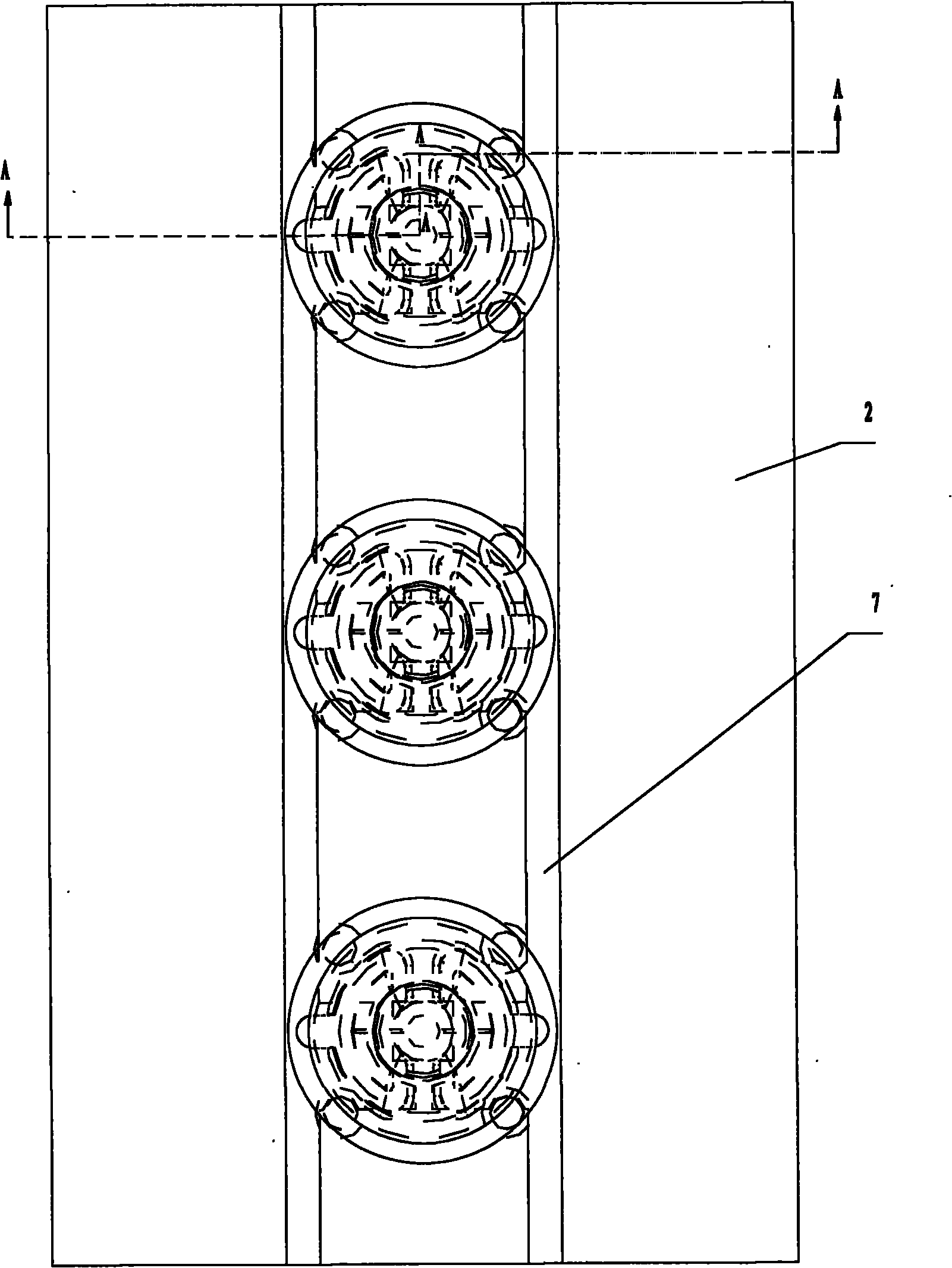
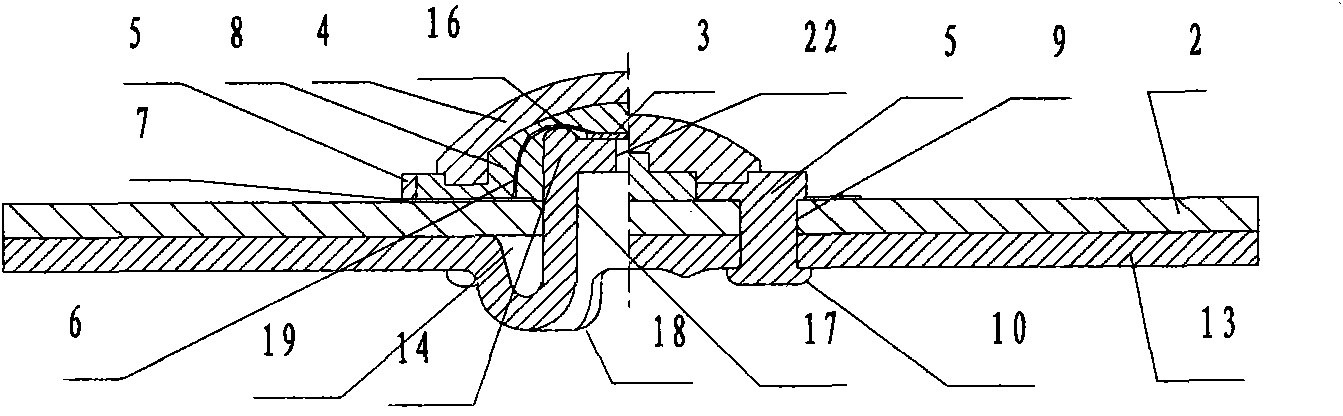
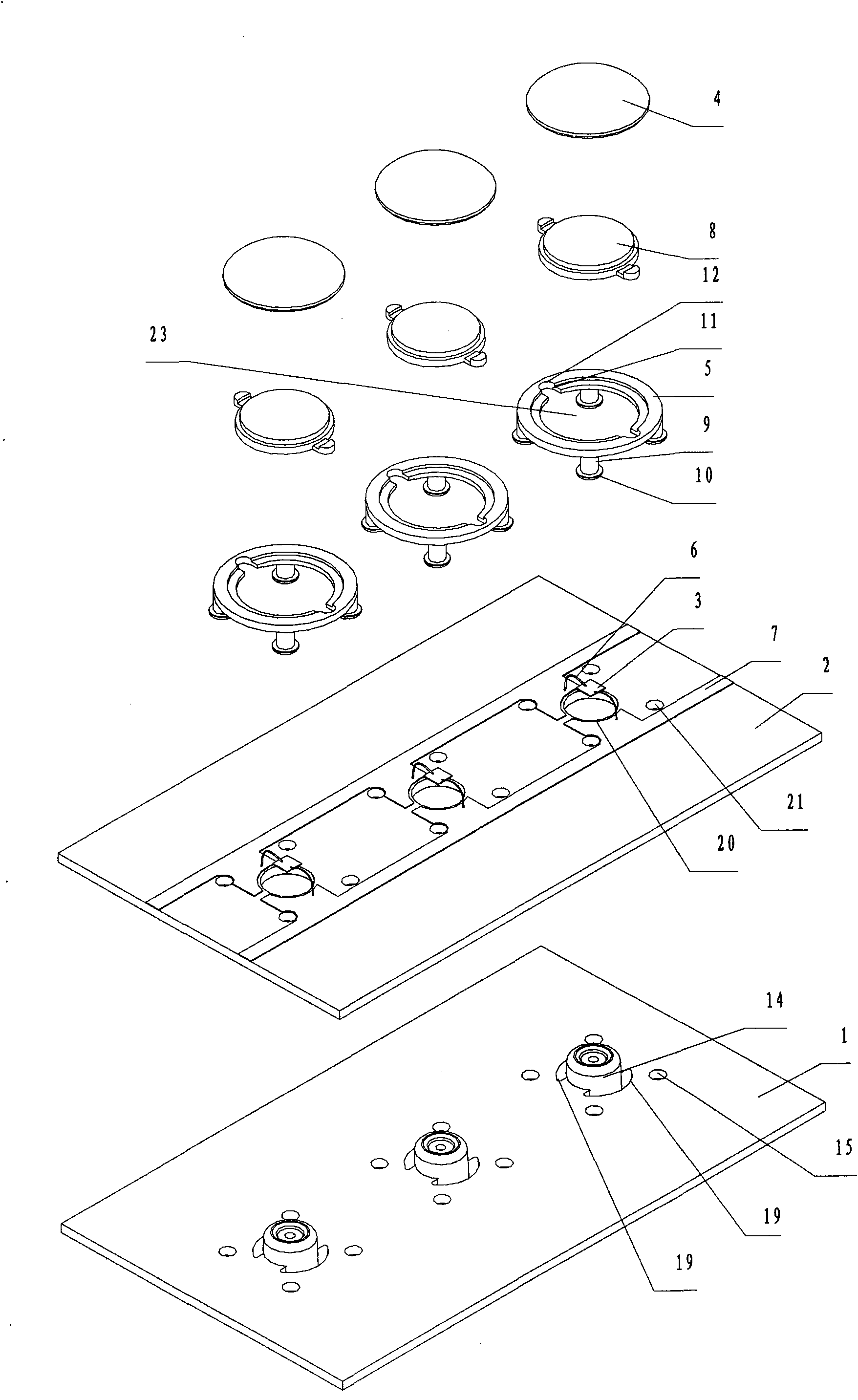
[0094] like Figure 1 to Figure 4 As shown, an LED integrated structure includes a heat dissipation substrate 1, a PCB board 2, an LED chip 3, a lens 4, a lens positioning ring 5, a gold wire 6 electrically connected to an electrode of the LED chip 3, and a layout of the electrically connected gold wire 6 The circuit conductive layer 7 is used for encapsulating the LED chip 3 and the encapsulant 8 of the gold wire 6 . Lens positioning ring 5 selects high-temperature-resistant PPA plastics for use.

[0095] The lens positioning ring 5 is provided with the first through hole 23 for positioning the lens 4 and the encapsulating colloid 8, and the lens positioning ring 5 is extended with a fixed column 9. At the end of the fixed column 9, the heat dissipation substrate 1 is placed on the A resisting portion 10 is formed in the mold for molding the lens positioning ring 5 when molding the plastic positioning ring. The lens positioning ring 5 is provided with a glue injection chann...

Embodiment 2

[0110] like Figure 1 to Figure 4 As shown, different from Embodiment 1, the manufacturing method of the LED integrated structure includes:

[0111] 1) The lens positioning ring 5 is injection-molded, and the fixing column 9, the glue port 12 and the injection channel 11 extending from one end surface of the lens positioning ring 5 are formed at the same time, and the length of the fixing column 9 is longer than the heat dissipation substrate 1 and the PCB board 2 The sum of the thickness;

[0112] 2) On the heat dissipation substrate 1, the chip fixing boss 14 on the heat dissipation substrate 1, the large hole 17 of the heat dissipation step through hole, the heat dissipation rib 18, the heat insulation blind hole 19 in the heat dissipation rib 18, and the lens positioning are formed by stamping The second through hole 15 fitted with the fixing column 9 of the ring 5;

[0113] 3) Small holes 22 connected to the large holes 17 of the heat dissipation step through holes formed...

Embodiment 3

[0124] like Figure 5 As shown, the difference from Embodiment 1 is that an LED integrated structure includes a heat dissipation substrate 50, an LED chip 51, a lens 52, a lens positioning ring 53, a wire 54 electrically connected to an electrode of the LED chip 51, and a wiring for electrically connecting the wire 54. The conductive layer 55 of the circuit shown in the figure is used for encapsulating the LED chip 51 and the encapsulant 56 of the wire 54 . The lens positioning ring 53 selects high temperature resistant PPO+GF plastics, and the number of lens positioning rings is six. There are no heat dissipation ribs and heat insulation blind holes on the heat dissipation substrate 50 .

[0125] The heat dissipation substrate 50 is made of high thermal conductivity ceramics or the like by die-casting. The layout circuit conductive layer 55 is directly disposed on the heat dissipation substrate 50, and the layout circuit conductive layer 55 is distributed on the same plane....


PUM


Abstract

The invention discloses a manufacture method of an LED integrated structure, comprises the following process steps: molding a heat dissipation substrate; molding a layout circuit conducting layer; molding a position lens or the plastic part of the lens; carrying out die bonding; electrically connecting an LED chip with the layout circuit conducting layer; and packaging the LED chip and wires. Themethod has the advantages of less process, simple technology, low manufacturing cost, small heat resistance and good heat dissipation of the intermediate link of manufacturing the LED chip and accurate position relation of the lens and the chip, and the LED integrated structure has the advantages of high luminous flux, simple structure, simple assembling, good heat dissipation effect and good optical effect.

Description

technical field [0001] The invention relates to a method for manufacturing an LED integrated structure used for lighting, backlight source modules, televisions, LED dot matrix display screens, projection equipment, etc., in particular to a method for manufacturing a high-power LED integrated structure. Background technique [0002] Semiconductor LED is a new type of solid light source. Its traditional packaging is an in-line structure such as epoxy resin encapsulating the LED chip and the pins are electrically connected to the LED chip. In the 1980s, surface mount technology began to be used. LED light sources, especially high-power LED light sources, concentrate heat when emitting light. If the heat generated by the LED chip is not dissipated in time, the temperature of the LED light source will be too high, which will lead to reduced light efficiency and short life of the LED. The rapid and effective dissipation of the heat generated by LED chips when they emit light has b...

Claims


Application Information

Patent Timeline
IPC IPC(8): F21V29/00F21V17/00F21Y101/02F21V19/00H01L33/48H01L25/03F21V23/06H01L33/64H01L33/54F21S2/00
CPCH05K3/00H05K2201/10106F21V17/00H05K2203/0323F21V23/06H01L2224/48111H01L2924/0002F21Y2101/02F21S2/00F21V5/04H01L25/03F21V19/00F21V17/005H01L33/64H05K1/021F21V29/00H01L2224/48091F21Y2105/001H01L33/48H01L33/54F21Y2105/10F21Y2115/10H01L2924/00014
Inventor 杨东佐
Owner 杨东佐
Why Eureka
Try Eureka