Check patentability & draft patents in minutes with Patsnap Eureka AI!

Capacitor substrate structure

A technology of capacitor substrate and dielectric layer, which is used in capacitors, fixed capacitors, components of fixed capacitors, etc.

Inactive Publication Date: 2011-02-02
IND TECH RES INST
View PDF6 Cites 12 Cited by
  • Summary
  • Abstract
  • Description
  • Claims
  • Application Information

AI Technical Summary

Problems solved by technology

[0009] Taiwan patent I 594811 mentions a laminate for forming a capacitance layer and a manufacturing method thereof, the structures of which are electrode copper layer / alumina barrier layer / modified alumina layer / aluminum, nickel, chromium bonding Metal layer / electrode copper layer, but capacitive substrate cannot be manufactured by printed circuit board process

Method used


Image

  • Capacitor substrate structure
  • Capacitor substrate structure
  • Capacitor substrate structure

Examples


Embodiment approach

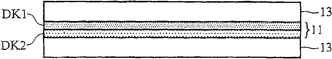
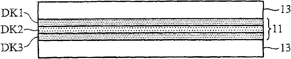
[0029] Such as figure 1 As shown, the capacitive substrate structure of the present invention includes an insulating layer 11 sandwiched between two conductive layers 13 . The thickness of the insulating layer 11 is approximately between 3 μm and 60 μm. If the insulating layer 11 is too thick, it will be difficult to effectively increase the capacitance density; but if the insulating layer 11 is too thin, the adhesion of the dielectric layer to the conductor layer will be poor, and the breakdown voltage will also decrease. The insulating layer 11 is divided into a first dielectric layer DK1 and a second dielectric layer DK2 with a high dielectric constant (at least greater than 45), and the dielectric constant of the second dielectric layer DK2 is higher than that of the first dielectric layer DK1 . In one embodiment of the present invention, the first dielectric layer DK1 includes organic resin. In another embodiment of the present invention, the first dielectric layer DK1 ...

Embodiment 1

[0042] The following is the preparation process of the capacitor substrate of the present invention.

[0043] Take bisphenol-A epoxy resin (bisphenol-Adiglycidyl ether) (188EL, Changchun Resin Company, Taiwan) and tetrabromo bisphenol-A epoxy resin (tetrabromo bisphenol-A diglcidyl ether) of different weights as shown in Table 1 respectively. ether) (BEB-350, Changchun Company, Taiwan), cyclo aliphatic epoxy (HP-7200, DIC, Japan), multifunctional epoxy resin (Multifunctional epoxy), and add 10ml of DMF , heated to 90 ° C ~ 95 ° C to completely dissolve the above resin. Get diamine (diaminodiphenyl sulfone, Diaminodiphenyl sulfone, DDS, available from ACROS, U.S.) of different weights as shown in Table 1 as hardening agent, and boron trifluoride mono-ethylamine (Boron trifluoride mono-ethylamine , BF3-MEA, purchased from ACROS, the United States) as a catalyst, was added to the above epoxy resin solution. After the hardener and catalyst are completely dissolved in the epoxy r...


PUM

PropertyMeasurementUnit
particle diameteraaaaaaaaaa

Abstract

The invention provides a capacitor substrate structure which can effectively solve the problems of high-leakage current and low insulation resistance of ultrahigh dielectric organic / inorganic blending substrate materials. An insulation layer arranged between two conductive layers is a multi-layer dielectric layer structure, wherein at least one dielectric layer is a high dielectric layer comprising mixture of high dielectric ceramic powder and conductive powder evenly dispersed in organic resin, and the other dielectric layers are ordinary organic resin and further comprise high dielectric ceramic powder. The insulation resistance of the capacitor substrate under the operation voltage is greater than 50K ohm and the leakage current is less than 100uAmp.

Description

【Technical field】 [0001] This invention relates to capacitive substrate structures, and more particularly to the composition of insulating layers in such structures. 【Background technique】 [0002] Recently, with the increasing demand for daily life and high functionality of electronic products, the soft electronics industry is booming. Electronic products also combine hard products with soft components to improve product functions and convenience. Electronic products are also developing towards thinner, flexible and high-speed and high-frequency signal transmission, so the ratio of passive components to active components on electronic substrates has also increased significantly, and the development of embedded passive components Technology can reduce the area of ​​circuit boards, increase the density of components used, and greatly improve the pass rate and reliability of products, which has become an inevitable trend. Among them, capacitive components are used the most, a...

Claims


Application Information

Patent Timeline
Patent Type & Authority Applications(China)
IPC IPC(8): H01G4/06H01G4/00H01G4/12
Inventor 刘淑芬陈孟晖陈碧义陈云田
Owner IND TECH RES INST
Features
  • R&D
  • Intellectual Property
  • Life Sciences
  • Materials
  • Tech Scout
  • Unparalleled Data Quality
  • Higher Quality Content
  • 60% Fewer Hallucinations
Learn More