Edge terminal structure of high-voltage power semiconductor device

A technology for power semiconductors and edge terminals, applied in semiconductor devices, electric solid state devices, electrical components, etc., can solve the problems of increasing chip cost, increasing chip area, etc., reducing chip cost, reducing electric field strength, and reducing breakdown voltage. improved effect

Inactive Publication Date: 2011-02-09
ZHEJIANG UNIV +1
View PDF1 Cites 28 Cited by
  • Summary
  • Abstract
  • Description
  • Claims
  • Application Information

AI Technical Summary

Problems solved by technology

Generally speaking, the withstand voltage will increase with the increase of the number of field limiting rings. However, the increase in the number of field limiting rings will also increase the occupied chip area, which will increase the cost of the chip.

Method used


Image

  • Edge terminal structure of high-voltage power semiconductor device
  • Edge terminal structure of high-voltage power semiconductor device
  • Edge terminal structure of high-voltage power semiconductor device

Examples


Embodiment 1

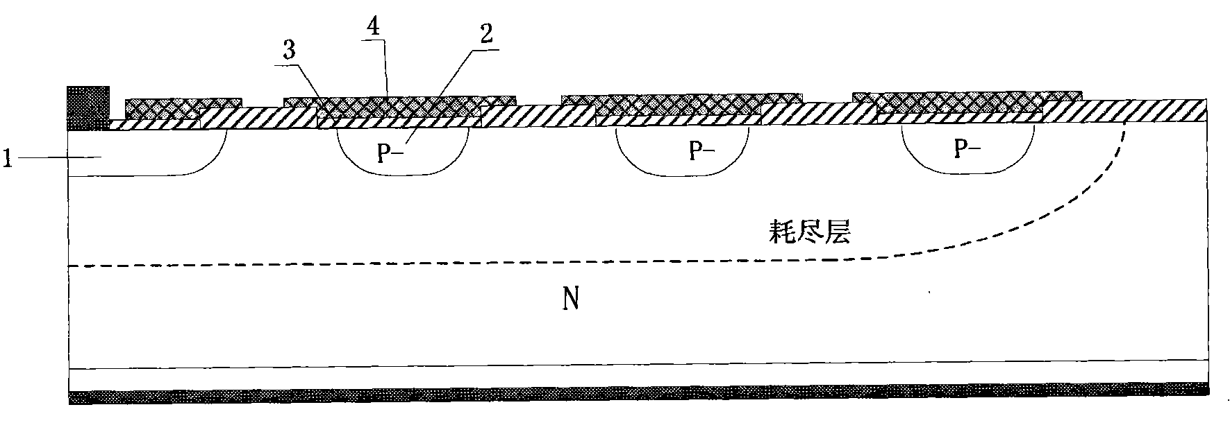
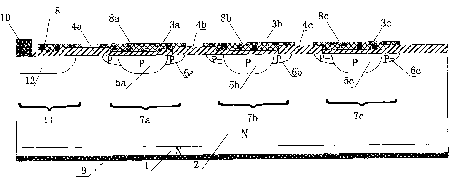
[0019] figure 2 A kind of embodiment of the present invention is provided, as shown in the figure, in arsenic ion (As) concentration is 5*10 22 cm -3 An epitaxial layer 2 of the same conductivity type is epitaxially grown on an N-type silicon substrate 1 (thickness 20 μm). The epitaxial layer 2 has a resistivity of 5Ω*cm and a thickness of 17 μm. A high-voltage power device 12 is provided on the upper surface of the epitaxial layer 2. The device can be VDMOS, LDMOS, BJT, etc. The device is composed of several cells connected in parallel. In the figure, only the edge area of ​​the edge cells is shown as its schematic diagram . An electrode 10 and a field plate 8 are provided on the device 12, which are active regions 11 for realizing core functions of the chip. In addition, an electrode 9 is also provided on the bottom of the substrate 1 as an external electrode of the test chip.

[0020] A P-type doped region 5a is provided on the outside of the device 12 relative to the ...

Embodiment 2

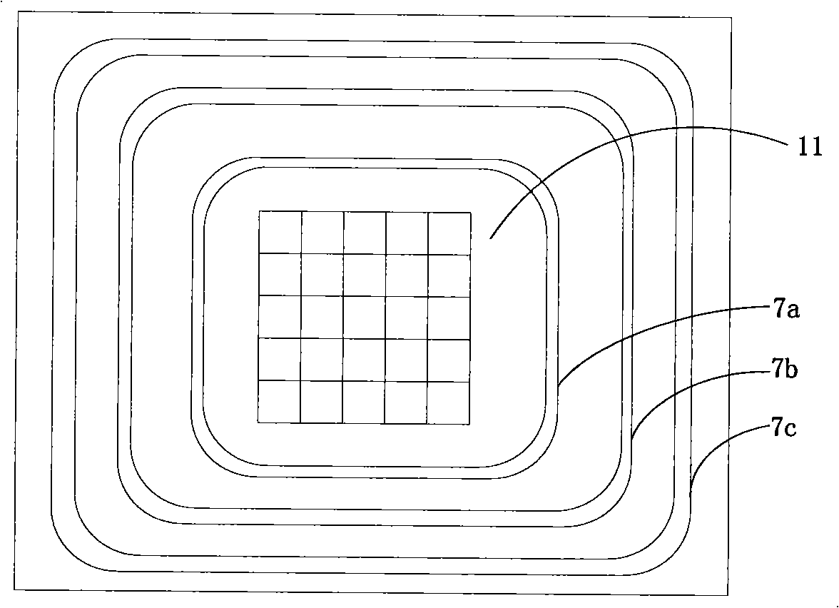
[0025] Such as Figure 4 As shown, the structure of this embodiment is similar to that of Embodiment 1, and instead of adding doped regions on both sides of the traditional field confinement ring, a doped region with a lower concentration is only added on the outside of the field confinement ring relative to the active region 11 , the junction depth of the doped region is 1-1.5 μm, and the field limiting ring 7a is 6 μm away from the active region. Adding an extra doped region only on one side of the field limiting ring can shorten the distance between the field limiting rings, from 8 to 10 μm in Example 1 to 6.5 to 7 μm, which reduces the chip area and reduces the cost. Compared with embodiment 1, this embodiment does not affect the effect of improving the breakdown voltage of edge cells. Figure 6 This example is given with figure 1 The comparison diagram of the electric field distribution of the traditional field confining ring is shown, in which, the left picture is fig...


PUM


Abstract

The invention discloses an edge terminal structure of a high-voltage power semiconductor device. The edge terminal structure comprises a plurality of field limiting rings which wind the power semiconductor device and have a conduction type opposite to that of a substrate; one or two side of each field limiting ring is provided with a doped region which has a conduction type the same as that of the field limiting ring and the doping concentration smaller than that of the field limiting ring; the field limiting rings are coated with field plates; and the field limiting rings and the field plates are separated by silicon dioxide layers. The material of the field plate can be selected from copper, aluminum, polysilicon, oxygen-doped polysilicon and the like. The doped regions with lower concentration are added around the conventional field limiting rings, so the intensity of electric field lines of an edge cellular can be effectively reduced, the electric field strength borne by the edge cellular is reduced, the breakdown voltage is improved, the area efficiency of the edge terminal structure is effectively improved, the chip area is saved, and the chip cost is reduced.

Description

technical field [0001] The invention relates to the technical field of semiconductor devices, in particular to an edge terminal structure of a high-voltage power semiconductor device. Background technique [0002] Power semiconductor devices, such as vertical double diffused field effect transistor (VDMOS), insulated gate bipolar transistor (IGBT), etc., are often composed of several cells connected in parallel in order to obtain a certain current capability. Since cell-to-cell depletion is formed among each other, breakdown is not easy to occur. However, the edge cell (also known as the transition region or the main junction) has dense electric field lines due to the small curvature radius of the depletion layer edge, and its electric field strength is much higher than that in the body, so the breakdown voltage will be much lower than in the body, and the breakdown first Occurs on the surface of edge cells. Therefore, a special structure should be adopted to protect the e...

Claims


Application Information

Patent Timeline
Patent Type & Authority Applications(China)
IPC IPC(8): H01L27/02H01L29/06
CPCH01L29/0619H01L29/0696H01L29/7811
Inventor 胡佳贤韩雁张世峰张斌
Owner ZHEJIANG UNIV
Why Eureka
Try Eureka