

Black silicon passivation method
A technology of black silicon and passivation film, applied in chemical instruments and methods, silicon compounds, inorganic chemistry, etc., can solve the problems of many dangling bonds, difficulty in black silicon passivation, and lower conversion efficiency of solar cells, so as to improve conversion efficiency , the effect of reducing the density of states
- Summary
- Abstract
- Description
- Claims
- Application Information
AI Technical Summary
Problems solved by technology
Method used
Image

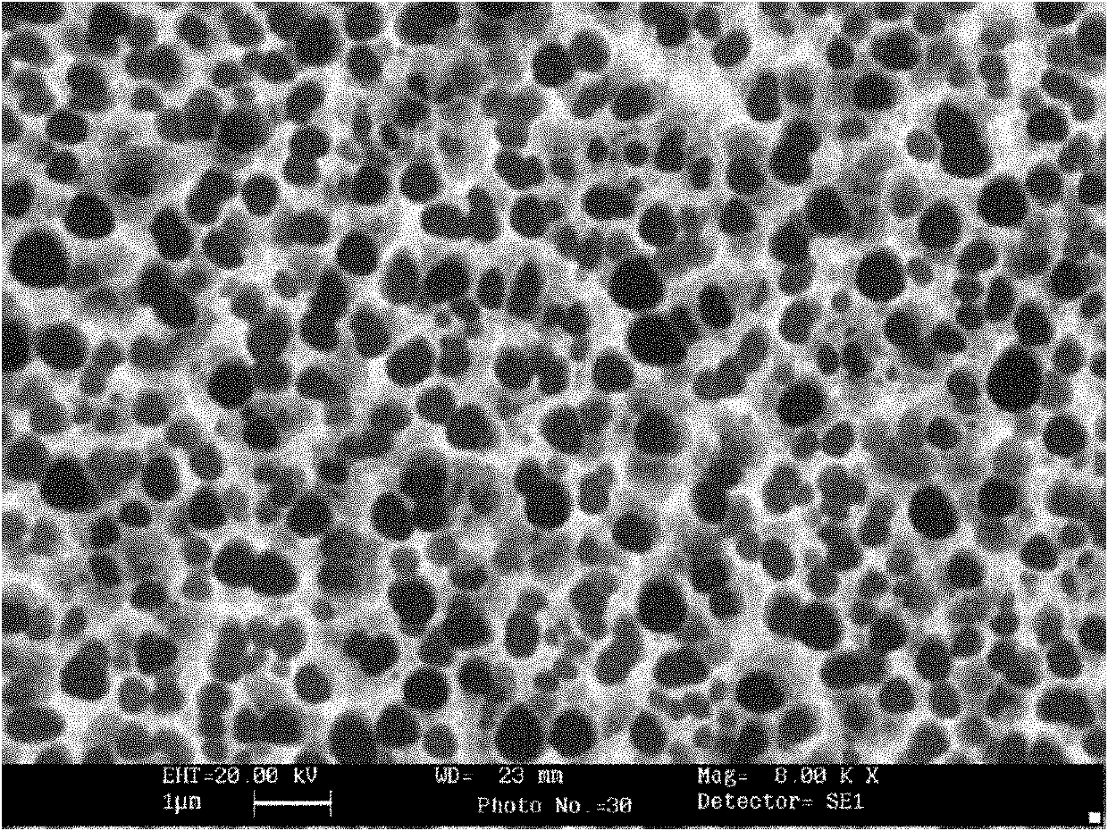
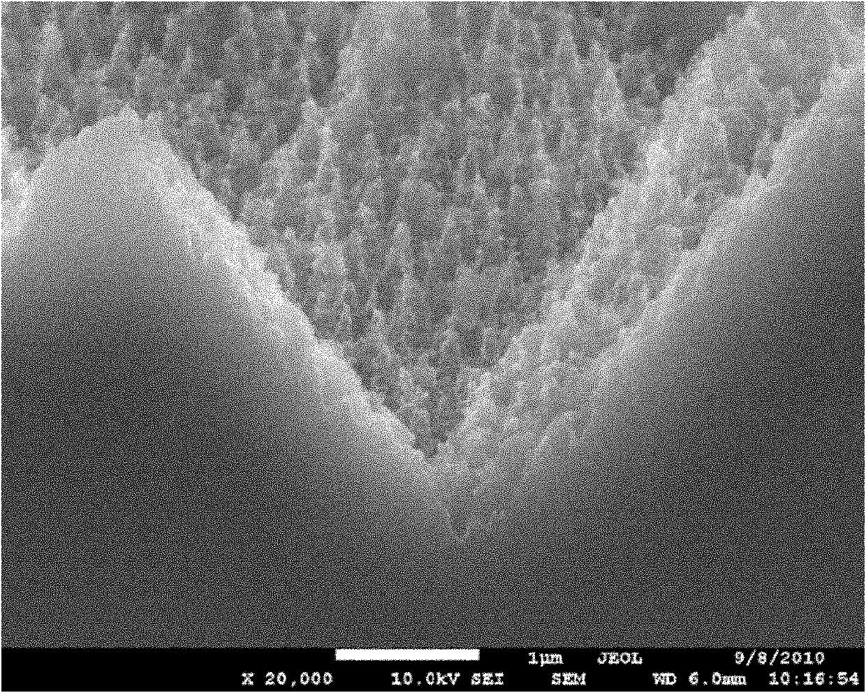
Examples
Embodiment Construction
[0029] The technical solution of the present invention will be described in detail below in conjunction with the accompanying drawings and embodiments.
[0030] Plasma enhanced chemical vapor deposition (Plasma Enhanced Chemistry Vapor Deposition, PECVD) is to place the sample on the sample stage in the deposition chamber, enter the process gas in the chamber, and generate plasma by gas glow discharge under the action of the plasma power supply , in the plasma atmosphere, the reactive gas is more easily decomposed, dissociated and ionized, thereby increasing the activity of the reactant, and the product is adsorbed on the surface of the sample, and deposited to form a thin film.
[0031] The present invention utilizes PECVD growth film to carry out the main mechanism of black silicon passivation to be: the mixed gas that feeds in the deposition chamber discharges under the action of plasma power supply to generate plasma, and the reaction gas in the mixed gas is as silane (SiH ...
PUM
 Abstract
Description
Claims
Application Information