
Device for thin film overlying photovoltaic and quick thermal treatment method

A rapid heat treatment and device technology, applied in the direction of electrical components, semiconductor devices, circuits, etc., can solve the problems of expensive crystal materials, not being able to use for a long time, and low technology

Inactive Publication Date: 2011-04-20
CM MFG
View PDF6 Cites 4 Cited by
  • Summary
  • Abstract
  • Description
  • Claims
  • Application Information

AI Technical Summary

Problems solved by technology

However, crystalline materials are usually expensive and difficult to manufacture on a large scale
Furthermore, devices made from such crystalline materials often have low technology to form thin films of photosensitive materials used to convert electromagnetic radiation into electricity
Similar limitations exist for the use of thin-film technology in the manufacture of solar cells, i.e., the efficiency is generally poor
In addition, the reliability of the membrane is generally poor, and it cannot be used for a long time in ordinary environmental applications
Often thin films are difficult to mechanically integrate with each other

Method used


Image

  • Device for thin film overlying photovoltaic and quick thermal treatment method
  • Device for thin film overlying photovoltaic and quick thermal treatment method
  • Device for thin film overlying photovoltaic and quick thermal treatment method

Examples


Embodiment Construction

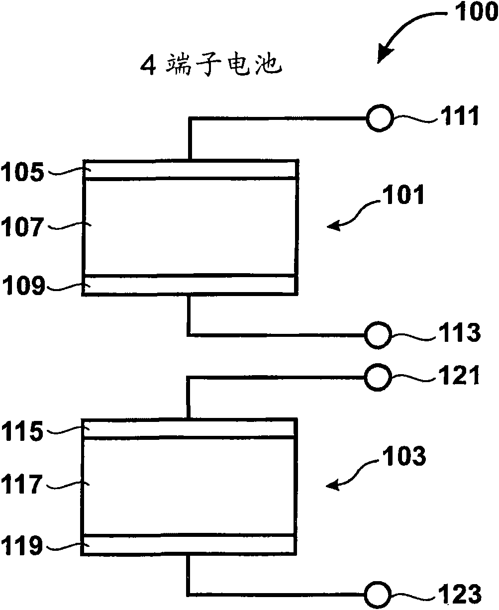
[0017] According to an embodiment of the present invention, a method and structure for forming a semiconductor material for photovoltaic applications is provided. More specifically, the present invention provides a method for fabricating a thin film photovoltaic device that can be used in tandem cell configurations as well as in other cell configurations. By way of example only, the method is used to provide copper indium disulfide thin film material for high efficiency solar cell applications. However, it should be understood that the present invention has a wider range of applications. For example, the embodiments of the present invention can be used to form other semiconductor thin films or include iron sulfide, calcium sulfide, zinc selenide, etc., and such as zinc oxide, iron oxide, copper oxide, etc. multilayer structure of metal oxides.

[0018] figure 1 is a simplified diagram of a tandem photovoltaic cell according to an embodiment of the invention. The illustratio...


PUM

PropertyMeasurementUnit
energyaaaaaaaaaa
thicknessaaaaaaaaaa
thicknessaaaaaaaaaa

Abstract

The invention discloses a device for thin film overlying photovoltaic and quick thermal treatment method so disposed that the method comprises a transparent substrate including a surface region. A first electrode layer overlies the surface region. A copper layer is formed overlying the first electrode layer and indium layer is formed overlying the copper layer to form a multi-layered structure. The multi-layered structure is subjected to a thermal treatment process in an environment containing a sulfur bearing species to form a bulk copper indium disulfide. the quick thermal treatment employing a gradient ranging between 1 degree centigrade per second to about 50 degrees centigrade per second. In specific embodiment, the resistivity of the first transparent electrode layer is kept of about 10 ohm / cm2 or less, and the light transmission rate is more than 80 percent.

Description

technical field [0001] The present invention generally relates to photovoltaic materials and methods of manufacture. More specifically, the present invention provides a method and structure for fabricating high efficiency thin film photovoltaic cells. By way of example only, the present methods and materials include absorber materials composed of copper indium disulfide, copper tin sulfide, iron disulfide, or other substances for single junction cells or multi-junction cells. Background technique [0002] From the beginning, human beings have been faced with the challenge of finding ways to use energy. Energy exists in forms such as petrochemical, hydroelectric, nuclear, wind, biomass, solar and more primitive forms such as wood and coal. Over the past century, modern civilization has relied on fossil energy as a vital source of energy. Petrochemical energy includes natural gas and oil. Natural gas includes lighter forms such as butane and propane, which are commonly use...

Claims


Application Information

Patent Timeline
Patent Type & Authority Applications(China)
IPC IPC(8): H01L31/18
CPCY02P70/50
Inventor 霍华德·W·H·李
Owner CM MFG
Learn More