Tapered photonic crystal quantum cascade laser and manufacture method thereof

A technology of photonic crystal and quantum cascade, which is applied in the direction of semiconductor lasers, lasers, phonon exciters, etc., can solve the problems of low output power, complex technology, large waveguide loss, etc., achieve low requirements for equipment and improve far field characteristics, the effect of increasing the output power

Inactive Publication Date: 2011-05-11
INST OF SEMICONDUCTORS - CHINESE ACAD OF SCI
View PDF3 Cites 32 Cited by
  • Summary
  • Abstract
  • Description
  • Claims
  • Application Information

AI Technical Summary

Problems solved by technology

[0003] In order to meet the applications in the above various fields, quantum cascade lasers are required to work in room temperature continuous wave single-mode, but so far, only a few quantum cascade lasers with individual wavelengths have achieved room temperature continuous wave single-mode operation. Quantum cascade lasers all use technologies such as electron beam exposure, buried grating, and secondary MOCVD epitaxy, which are not only expensive but also technically complex, which makes the development process of quantum cascade lasers extremely difficult, which is not conducive to improving device reliability and realizing mass production
The method of using the top grating (evenly distributing the grating on the top of the la

Method used


Image

  • Tapered photonic crystal quantum cascade laser and manufacture method thereof
  • Tapered photonic crystal quantum cascade laser and manufacture method thereof
  • Tapered photonic crystal quantum cascade laser and manufacture method thereof

Examples


Embodiment Construction

[0079] In order to make the object, technical solution and advantages of the present invention clearer, the present invention will be described in further detail below in conjunction with specific embodiments and with reference to the accompanying drawings.

[0080] In the following, the present invention will be further described by taking the InP / InGaAs / InAlAs material system and the tapered photonic crystal quantum cascade laser as examples, but this does not constitute a limitation to the present invention.

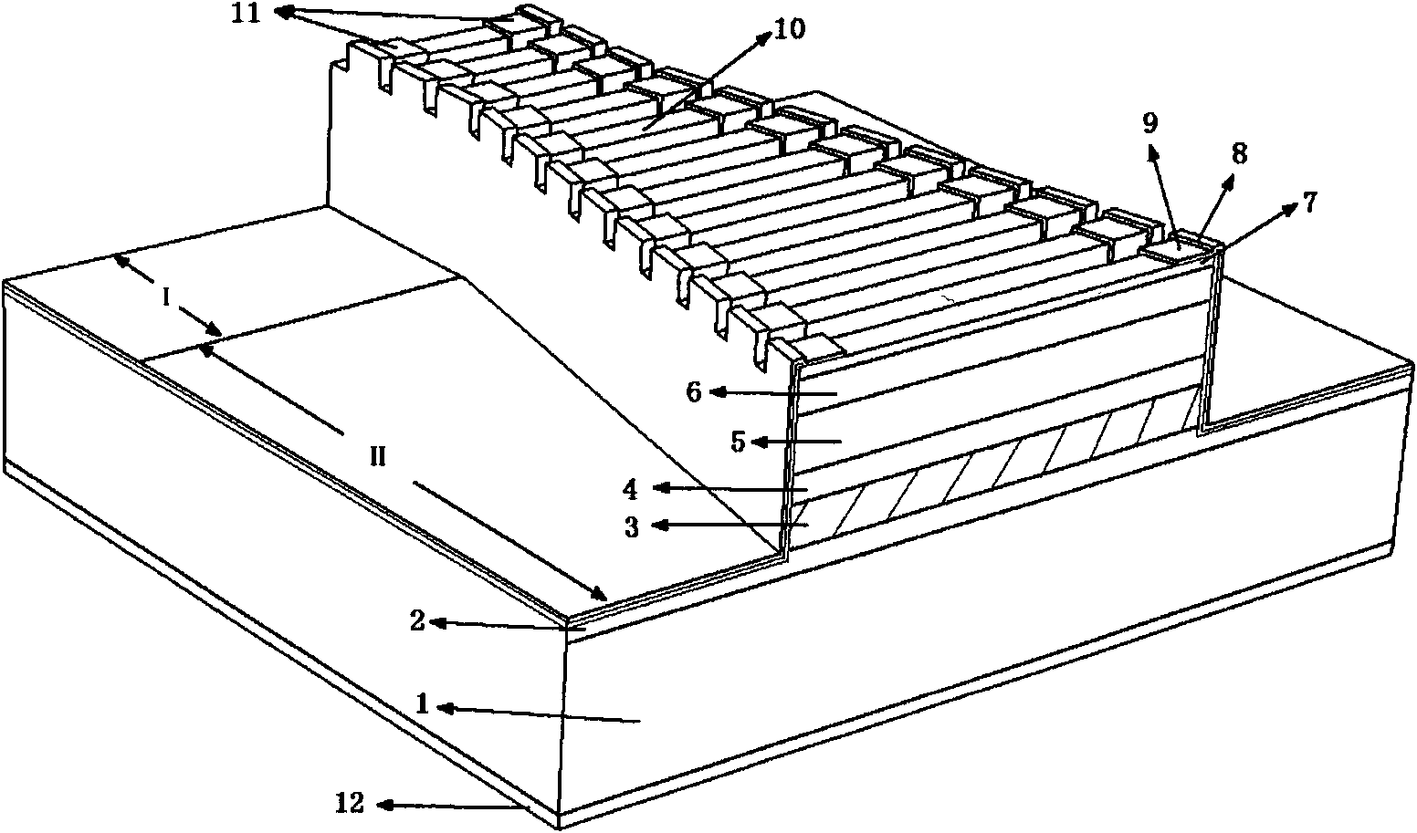
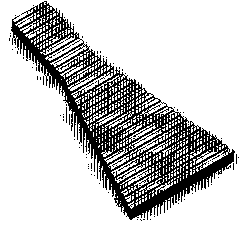
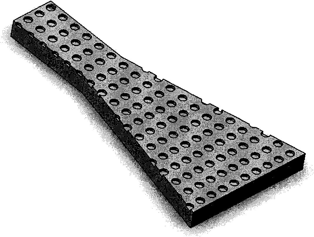
[0081] The invention provides a high-power, near-diffraction-limited tapered photonic crystal quantum cascade laser, which includes an n-type doped InP substrate, an InGaAs lower waveguide layer, a 35-level periodic active region, an InGaAs upper waveguide layer, and an InP upper waveguide layer. Cladding layer, InP upper cladding layer, highly doped InP ohmic contact layer, photonic crystal waveguide, double-groove ridge structure and tapered gain amplification region...


PUM

PropertyMeasurementUnit
Ridge widthaaaaaaaaaa
Lengthaaaaaaaaaa
Lengthaaaaaaaaaa

Abstract

The invention discloses a tapered photonic crystal quantum cascade laser for outputting near-diffraction-limited beams and the manufacture method thereof. The laser comprises a substrate, as well as a lower waveguide layer, an active area, an upper waveguide layer, an upper cover layer, an upper contact layer, an ohmic contact layer, an electrical insulation layer, a front side electrode and a rear side electrode on the substrate. The laser has the ridge-shaped mesa double-grooved waveguide structure, wherein the ridge-shaped mesa structure includes a main control oscillation area with a uniform ridge width and a gain amplification area with a tapered structure. The photonic crystal structure is used for providing a distributed feedback waveguide manufactured between the upper contact layer and the ohmic contact layer. The tapered photonic crystal quantum cascade laser can acquire singe-mode near-diffraction-limited beam output. The waveguide structure with the combination of the ridge-shaped mesa and the tapered gain amplification area can greatly reduce the far-field divergence angle, thereby improving the output power while obviating the heat dissipation problem that is difficult to avoid for the similar wide-ridge large-power devices.

Description

technical field [0001] The invention relates to the technical field of semiconductor optoelectronics, in particular to a high-power, near-diffraction-limited light output photonic crystal quantum cascade laser and a manufacturing method thereof. Background technique [0002] In 1994, Bell Labs first invented the quantum cascade laser working in the far infrared band. It is different from the traditional semiconductor laser. The quantum cascade laser is a unipolar device that only relies on the energy levels between subbands to participate in electronic transitions. People can pass Ingenious energy band structure design, without changing the material system, can adjust the lasing wavelength arbitrarily within a certain band range, breaking through the limitation that the lasing wavelength of traditional semiconductor lasers must depend on the band gap width of the material, and greatly expanding human The spectral range that can be used, therefore, the quantum cascade laser i...

Claims


Application Information

Patent Timeline
IPC IPC(8): H01S5/343H01S5/22H01S5/06
Inventor 张伟王利军刘俊岐李路张全德陆全勇高瑜刘峰奇王占国
Owner INST OF SEMICONDUCTORS - CHINESE ACAD OF SCI
Why Eureka
Try Eureka