Silicon carbide consubstantial PIN (Personal Identification Number) microstructure material and preparation method thereof

A manufacturing method and technology of silicon carbide, applied in semiconductor/solid-state device manufacturing, electrical components, circuits, etc., to achieve the effects of improving switching speed, high power density, and bright surface

Inactive Publication Date: 2011-05-18
INST OF SEMICONDUCTORS - CHINESE ACAD OF SCI
View PDF2 Cites 7 Cited by
  • Summary
  • Abstract
  • Description
  • Claims
  • Application Information

AI Technical Summary

Problems solved by technology

[0005] The existing technology uses a sudden N between the I-type layer and the N-type substrate. - The buffer layer, that is, a small amount of N-type dopant is introduced during the epitaxial buffer layer, and then the N-type dopant is turned off for I-type layer epitaxy, which makes the gap between the N-type substrate and the buffer layer, and between the buffer layer and the I-type layer doping mutation

Method used


Image

  • Silicon carbide consubstantial PIN (Personal Identification Number) microstructure material and preparation method thereof
  • Silicon carbide consubstantial PIN (Personal Identification Number) microstructure material and preparation method thereof
  • Silicon carbide consubstantial PIN (Personal Identification Number) microstructure material and preparation method thereof

Examples


Embodiment

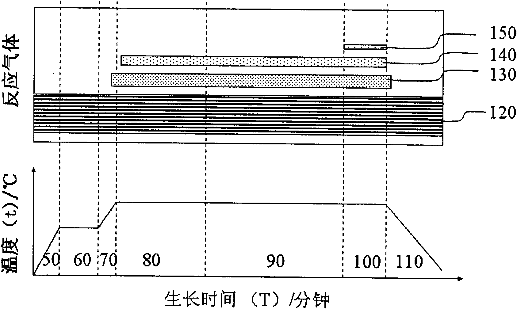
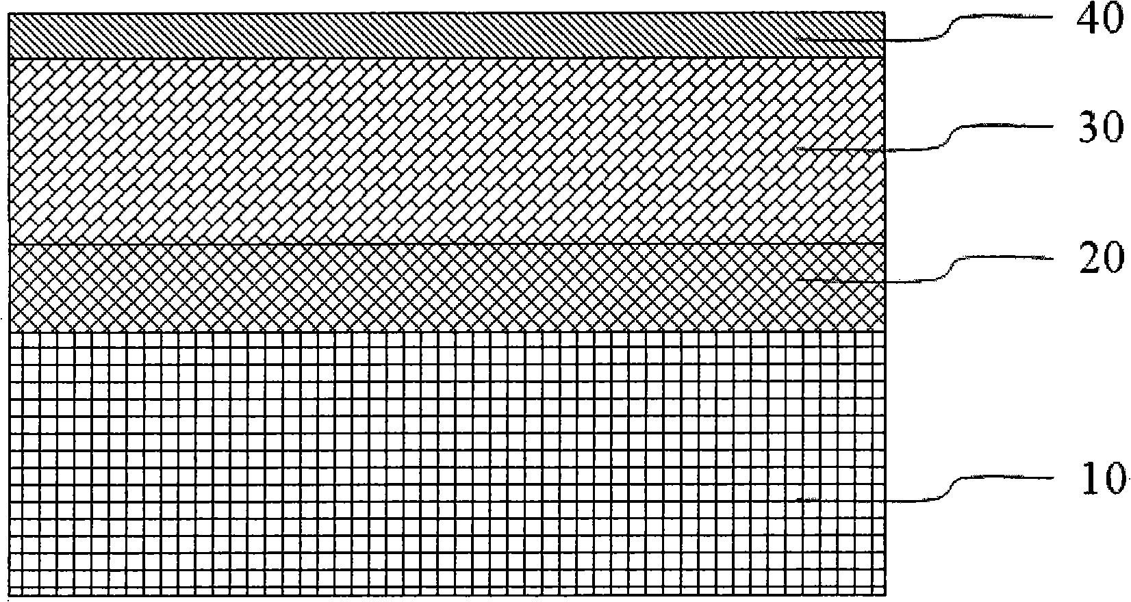
[0048] A single crystal 4H-SiC substrate is used, and its Si(0001) surface is 8° away from the direction. After chemical polishing, it is cleaned and placed in a low-pressure chemical vapor deposition equipment. Hydrogen gas is introduced to maintain a pressure of 40 Torr. , heat up to 1350° C. and keep it warm, etch and polish the surface of the substrate with hydrogen gas for 30 minutes. Then raise the temperature to 1500°C at a rate of 40°C / min, feed ethylene at a flow rate of 1 sccm, and when the substrate surface is heated to 1550°C, feed silane with a flow rate of 1 sccm, keep the temperature constant, grow for 180 minutes, and complete the buffer layer and the growth of the intrinsic layer. Keep the growth conditions unchanged, and carry out the P + Cap growth, time 3 minutes. Turn off borane, silane and ethylene in turn, and cool down naturally under a hydrogen atmosphere. The pressure was maintained at 40 Torr throughout the process, and the hydrogen flow rate was...


PUM

PropertyMeasurementUnit
thicknessaaaaaaaaaa
thicknessaaaaaaaaaa

Abstract

The invention discloses a silicon carbide consubstantial PIN (Personal Identification Number) microstructure material which comprises an N type silicon carbide substrate, an N-variable concentration buffer layer arranged on the N type silicon carbide substrate, an intrinsic layer arranged on the N-variable concentration buffer layer, and a P+ cap layer arranged on the intrinsic layer. The invention simultaneously discloses a preparation method of the silicon carbide consubstantial PIN microstructure material. The invention can prepare an extension SiC epitaxial material with the advantages ofbright surface and uniform resistivity, the background carrier concentration of the intrinsic epitaxial layer can be reduced to the 1015 order of magnitude, and the microstructure material provided by the invention is suitable for high-power electronic and electric devices of semiconductors.

Description

technical field [0001] The invention relates to the technical field of preparation of wide bandgap semiconductor epitaxy materials, in particular to a silicon carbide homogeneous PIN microstructure material and a manufacturing method thereof. Background technique [0002] Silicon carbide is an excellent wide-bandgap semiconductor material. It has high carrier mobility and breakdown electric field, good chemical inertness, high temperature resistance, and radiation resistance. It has great application potential in the field of high-power power electronics, so , it is of great practical significance to design and fabricate materials and devices based on homogeneous silicon carbide. [0003] In addition to the conventional PIN performance, the silicon carbide material of the PIN structure can also achieve higher power density and higher frequency switching speed according to the special design of the I-type intrinsic layer and the P+ cap layer. [0004] The existing method for...

Claims


Application Information

Patent Timeline
Patent Type & Authority Applications(China)
IPC IPC(8): H01L29/24H01L21/18
Inventor 孙国胜刘兴昉王雷赵万顺杨挺吴海雷闫果果曾一平李晋闽
Owner INST OF SEMICONDUCTORS - CHINESE ACAD OF SCI
Why Eureka
Try Eureka