Manufacturing method for nanowire with CuO/ZnO core/shell structure
A manufacturing method and nanowire technology, applied in the field of nanophotonics, can solve the problems of large lattice mismatch of ZnO crystals and difficult realization of nanowires, and achieve the effects of uniform diameter and length distribution, improved efficiency and low manufacturing cost.
- Summary
- Abstract
- Description
- Claims
- Application Information
AI Technical Summary
Problems solved by technology
Method used
Image
Examples
Embodiment
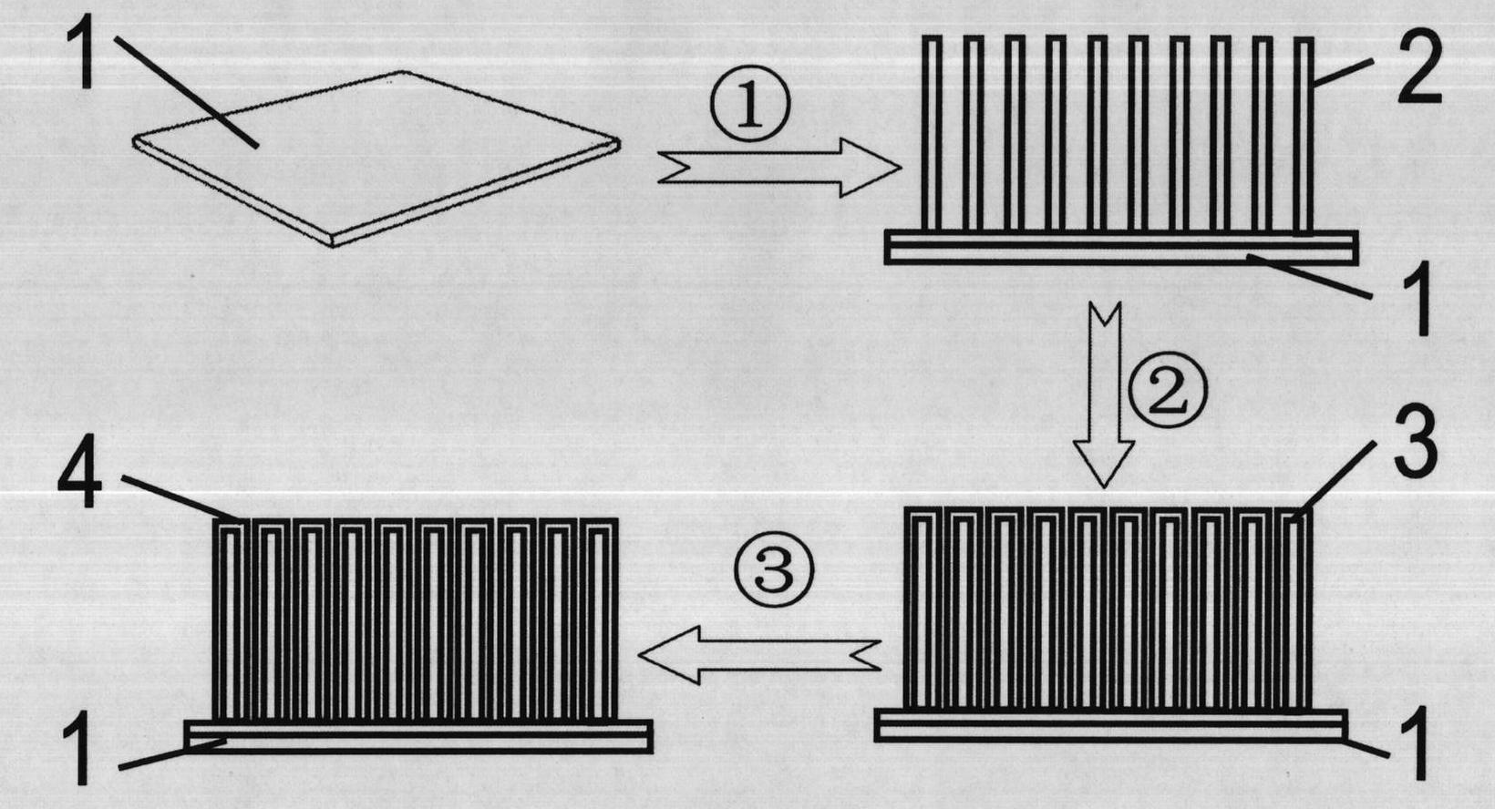
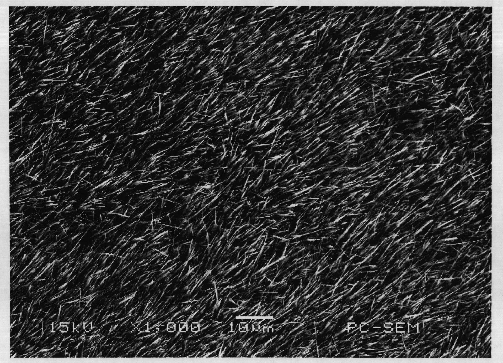
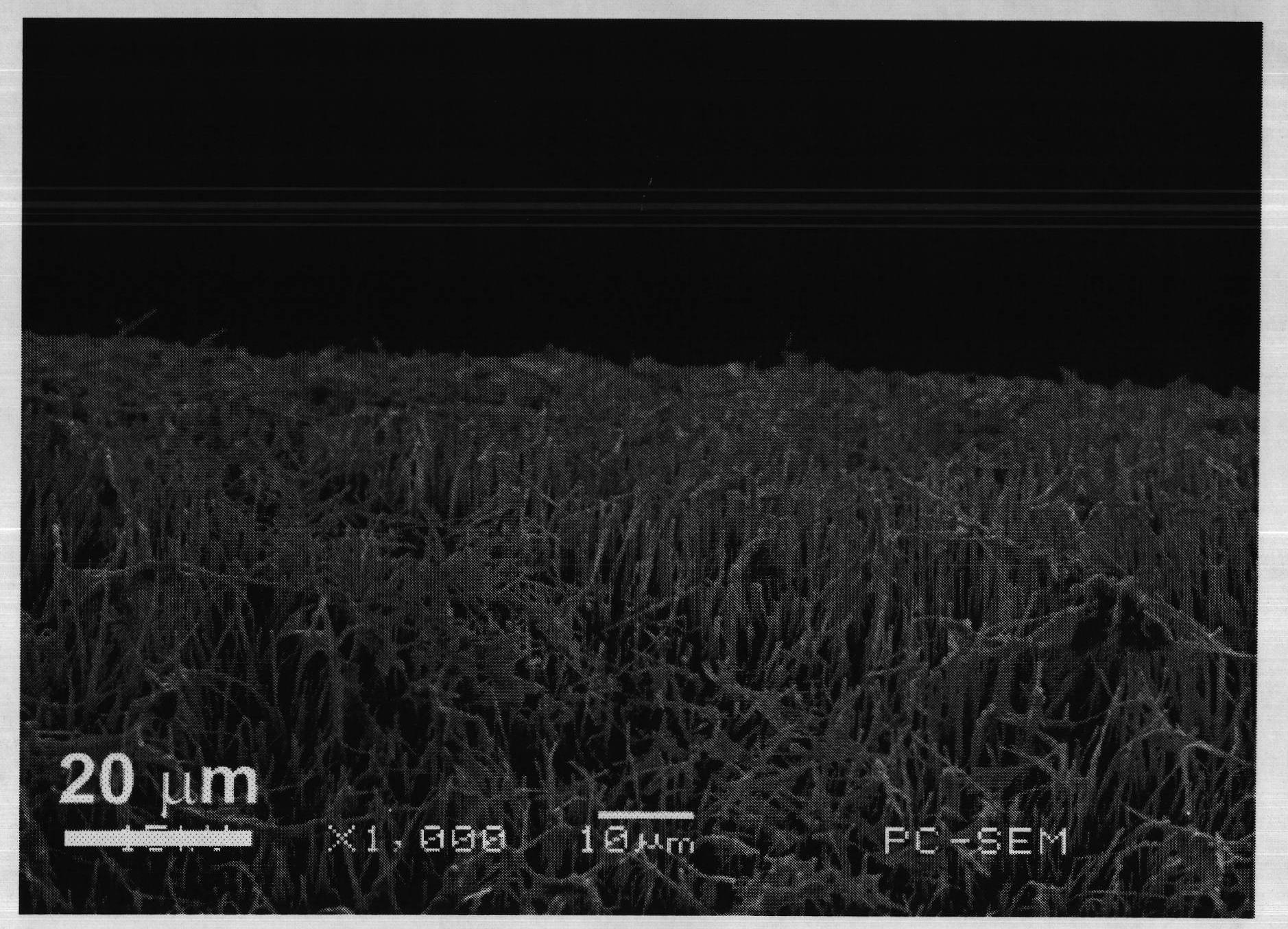
[0036] First, cut high-purity (99.9%) copper foil into small pieces of copper foil with a width of 10mm x 20mm length x 0.5mm thickness, flatten them with a glass or metal plate, and place the flat copper foil in alcohol and acetone at a volume of 1: Ultrasonic cleaning in a mixture of 1 ratio for 3 minutes to remove the dirt adhering to the surface, put the copper foil cleaned with alcohol and acetone into 1mol / L dilute hydrochloric acid solution for 3 minutes to remove the oxide on the surface, take out Afterwards, rinse with deionized water for several times, and then dry naturally in the air; secondly, attach the cleaned and dried copper foil to the quartz plate and place it on an electric furnace at 500°C for 4 hours in the air and then cool it rapidly to At room temperature, the CuO nanowire array was obtained; again, on the copper foil substrate on which the CuO nanowire array had been grown, drop 5 drops of an ethanol solution saturated with zinc acetate on the surface ...
PUM
 Abstract
Description
Claims
Application Information


