Method and system for forming Cu-In-Ga-S-Se absorption layer and cadmium sulfide buffer layer in antivacuum way

A copper indium gallium sulfide selenide and absorber layer technology, which is applied in sustainable manufacturing/processing, electrical components, climate sustainability, etc., can solve the problems of expensive manufacturing cost of equipment, many grain boundaries, and low material utilization rate.

Inactive Publication Date: 2011-07-20
JENN FENG NEW ENERY CO LTD
View PDF4 Cites 10 Cited by
  • Summary
  • Abstract
  • Description
  • Claims
  • Application Information

AI Technical Summary

Problems solved by technology

[0006] The manufacturing method of the above-mentioned copper indium gallium selenium solar cell can adopt vacuum process or non-vacuum process, wherein the vacuum process mainly uses sputtering method or evaporation method, although the product quality is better, but the material utilization rate is low, the equipment is expensive and the manufacturing The cost is high, and the ink process (InkProcess) is used instead of the vacuum process, which can grea

Method used


Image

  • Method and system for forming Cu-In-Ga-S-Se absorption layer and cadmium sulfide buffer layer in antivacuum way
  • Method and system for forming Cu-In-Ga-S-Se absorption layer and cadmium sulfide buffer layer in antivacuum way
  • Method and system for forming Cu-In-Ga-S-Se absorption layer and cadmium sulfide buffer layer in antivacuum way

Examples


Embodiment Construction

[0015] The implementation of the present invention will be described in more detail below in conjunction with the accompanying drawings, so that those skilled in the art can implement it after studying this specification.

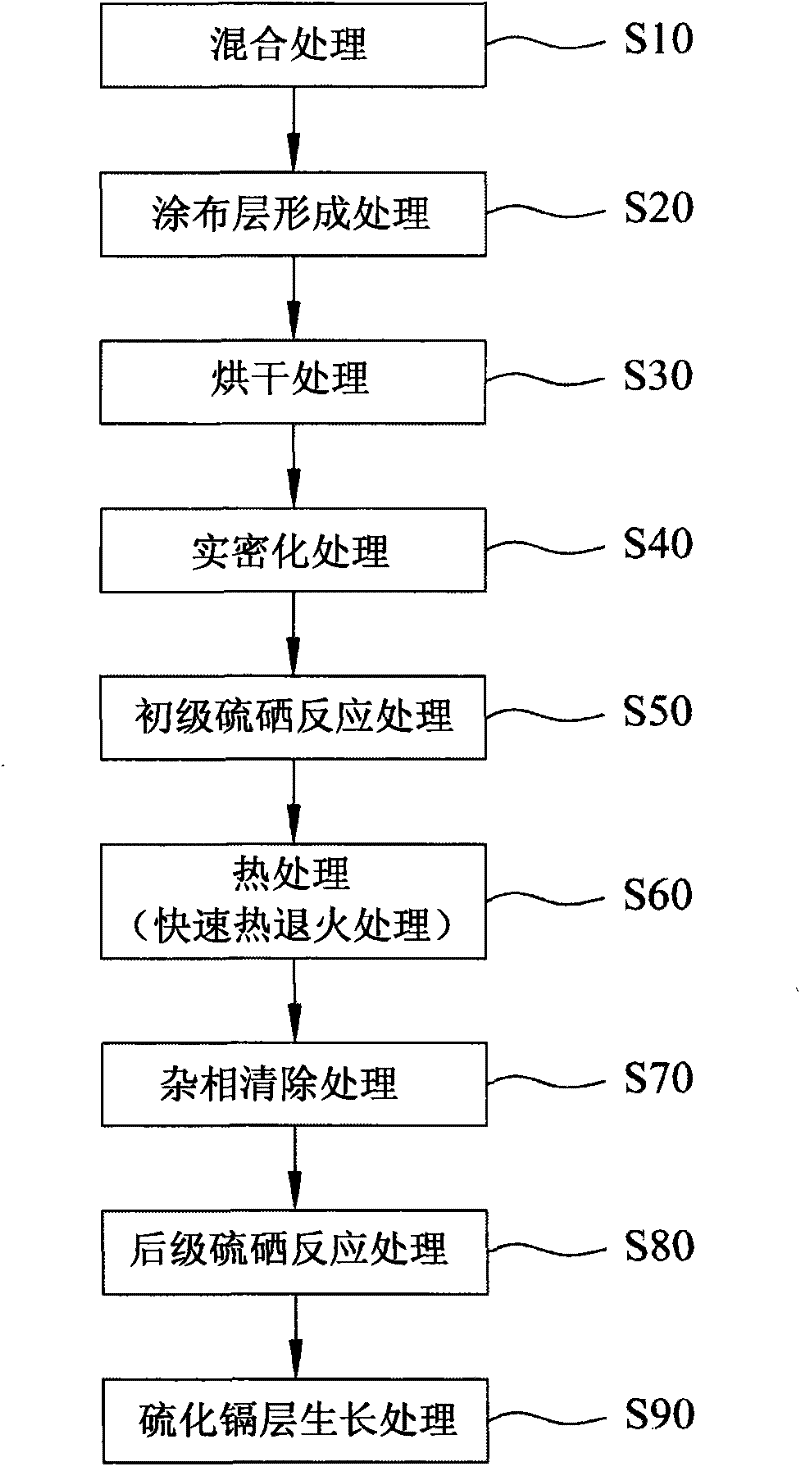
[0016] refer to figure 2 , a flowchart of the inventive method. Such as figure 2 As shown, the method of the present invention starts from step S10, and the mixing process is carried out under non-vacuum, including mixing copper indium gallium sulfide selenide powder, solvent and additives to form copper indium gallium sulfide selenide slurry, the copper indium gallium sulfide selenide powder The body can include copper indium alloy (CuIn), copper indium gallium compound (CuInGa), copper indium selenide (CuInSe), copper indium gallium selenide (CuInGaSe), copper indium sulfide (CuInS) and copper indium gallium sulfide (CuInGaS) powder The solvent may include at least one of alcohols and amines, and the additive may include at least one of dispersants, a...


PUM


Abstract

The invention discloses a method and system for forming a Cu-In-Ga-S-Se absorption layer and a cadmium sulfide buffer layer in an antivacuum way. The method comprises the steps of: in specific to a substrate with a back electrode layer under antivacuum, forming a coating layer from mixed slurry on the back electrode layer, primarily drying, compacting the coating layer by using a compacting device, carrying out primary S-Se reaction treatment to form a primary Cu-In-Ga-S-Se layer, thermally treating to improve the lattice matching of the primary Cu-In-Ga-S-Se layer, carrying out miscellaneous-phase removal treatment by using potassium cyanide or bromides to remove miscellaneous-phase cuprous selenide and copper sulphide, carrying out post-stage S-Se reaction treatment to generate a needed post-stage Cu-In-Ga-S-Se absorption layer, and finally, forming a cadmium sulfide buffer layer on the Cu-In-Ga-S-Se absorption layer by using a chemical-tank water bath method.

Description

technical field [0001] The invention relates to a method and system for forming a copper indium gallium sulfide selenide absorbing layer and a cadmium sulfide buffer layer, in particular, performing a two-stage sulfur selenide reaction in a non-vacuum environment to form an absorbing layer with good quality. Background technique [0002] Under the international trend of green energy, copper indium gallium selenide (CIGS) solar cells with quaternary compounds in thin film solar cells are not limited by raw materials, can be fabricated on large-area flexible substrates, and have the advantages of high conversion efficiency, especially The conversion efficiency of the unit battery (Cell) can reach 20% and the conversion efficiency of the module can reach 14%. Therefore, it has gradually attracted the attention of the new energy industry in various countries and is committed to its development. [0003] refer to figure 1 , is a schematic diagram of a CIGS solar cell in the prio...

Claims


Application Information

Patent Timeline
IPC IPC(8): H01L31/18
CPCY02P70/50
Inventor 庄泉龙
Owner JENN FENG NEW ENERY CO LTD
Why Eureka
Try Eureka