Outer gettering method for silicon wafer
A silicon wafer and silicon wafer surface technology, applied in the field of integrated circuits and solar energy applications, can solve problems such as reducing the photoelectric conversion efficiency of solar cells, and achieve the effects of improving the quality of silicon wafers, good gettering effect, and low cost
- Summary
- Abstract
- Description
- Claims
- Application Information
AI Technical Summary
Problems solved by technology
Method used
Image
Examples
Embodiment 1
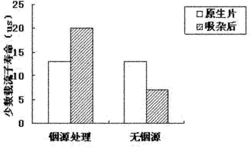
[0024] (1) Take a single crystal silicon wafer, the thickness is about 200 microns, and the minority carrier lifetime is about 13 μs after testing;
[0025] (2) Indium source (0.01mol / L InCl 3 solution) double-sided coating on the surface of single crystal silicon;
[0026] (3) Pass oxygen into the RTP-300 rapid heat treatment furnace, the gas flow rate is about 1L / min, and send the monocrystalline silicon wafer treated in step (2) into the furnace, and the furnace temperature is raised to 900°C at 50°C / s , after 3 minutes of heat preservation, cool down to room temperature with the furnace;
[0027] (4) Soak in hydrofluoric acid (10% by volume) for 30s to remove the surface glass layer.
Embodiment 2
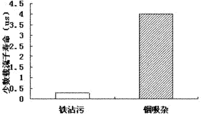
[0034] (1) Take a monocrystalline silicon wafer contaminated by iron impurities, the thickness is about 600 microns, and the minority carrier lifetime is about 0.3 μs after testing;
[0035] (2) Indium source (0.05mol / L of In 2 (SO 4 ) 3 solution) double-sided coating on the surface of single crystal silicon;
[0036] (3) Pass oxygen into a conventional heat treatment furnace, the gas flow rate is about 1L / min, and the temperature in the furnace rises to
[0037] 900°C, put the above-mentioned monocrystalline silicon wafer into the furnace, keep it warm for 120 minutes, and then cool down to room temperature with the furnace;
[0038] (4) Soak in hydrofluoric acid (10% by volume) for 30s to remove the surface glass layer.
[0039] figure 2 A comparison chart of minority carrier lifetimes of single crystal silicon wafers contaminated with iron impurities before and after treatment in Example 2 is given. Depend on figure 2 It can be seen that the minority carrier lifeti...
Embodiment 3
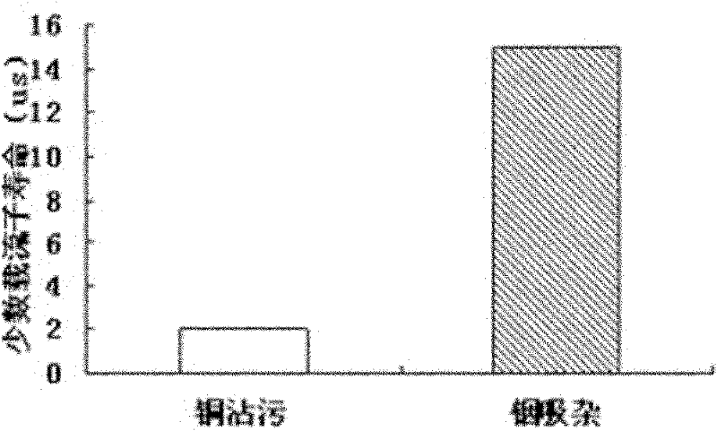
[0041] (1) Take a copper-contaminated single-crystal silicon wafer, the thickness is about 200 microns, and the minority carrier lifetime is about 2 μs after testing;
[0042] (2) Indium source (0.02mol / L In(NO 3 ) 3 solution) double-sided coating on the surface of single crystal silicon;
[0043] (3) Pass oxygen into the RTP-300 rapid heat treatment furnace, the gas flow rate is about 1L / min, and send the monocrystalline silicon wafer treated in step (2) into the furnace, and the furnace temperature is raised to 800°C at 50°C / s , after 6 minutes of heat preservation, cool down to room temperature with the furnace;
[0044] (4) Soak in hydrofluoric acid (10% by volume) for 30s to remove the surface glass layer.
[0045] image 3 A comparison chart of minority carrier lifetimes of single crystal silicon wafers contaminated with copper impurities before and after treatment in Example 3 is given. Depend on image 3 It can be seen that the minority carrier lifetime of the mo...
PUM
| Property | Measurement | Unit |
|---|---|---|
| thickness | aaaaa | aaaaa |
| thickness | aaaaa | aaaaa |
| thickness | aaaaa | aaaaa |
Abstract
Description
Claims
Application Information


