Eureka AIR delivers breakthrough ideas for toughest innovation challenges, trusted by R&D personnel around the world.

Method for manufacturing wafer-level patch panel

An adapter board and wafer-level technology, which is applied in semiconductor/solid-state device manufacturing, electrical components, circuits, etc., can solve problems such as low formation efficiency, difficulty in dielectric layer deposition, and limited application range of wafer-level packaging technology. Achieve the effect of realizing large-scale production, reducing process difficulty and process cost

Active Publication Date: 2011-08-17
JIANGYIN CHANGDIAN ADVANCED PACKAGING CO LTD
View PDF8 Cites 9 Cited by
  • Summary
  • Abstract
  • Description
  • Claims
  • Application Information

AI Technical Summary

Problems solved by technology

[0003] Limited by chip size and reliability, the application range of wafer-level packaging technology is still limited to some low-pin-count products
In the three-dimensional stacking technology, although wire bonding can achieve multi-layer stacking, the application of high-speed signal transmission modules is limited by the length and diameter of the wires, so the use of large areas is still in flash memory, smart cards, radio frequency identification, etc.
[0008] 1) Through-hole formation, the usual way of forming through-holes is to use deep reactive ion etching, so the formation efficiency is low, and due to the control factors of the etching process, the formed through-hole wall has a scallop structure;
[0009] 2) Difficulty in deposition of dielectric layer
In order to ensure the insulation between silicon and the through-hole metal, a dielectric layer needs to be deposited on the through-hole wall, but the deposition of the dielectric layer is very difficult due to the extremely small size of the through-hole;
[0010] 3) It is difficult to fill the through hole metal
Since the metal filling of the through hole is to pre-deposit the seed layer metal in the through hole, and then use the electroplating process, it is difficult to avoid the void defect in the through hole (the growth characteristic of the electroplated metal) in this way.
[0011] Based on the above three reasons, silicon-based interposer technology using TSV technology does not yet have mass production capacity

Method used


Image

  • Method for manufacturing wafer-level patch panel
  • Method for manufacturing wafer-level patch panel
  • Method for manufacturing wafer-level patch panel

Examples


Embodiment Construction

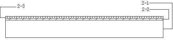
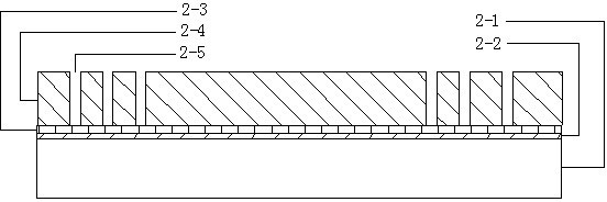
[0033] see Figure 1~Figure 11 , Figure 1~Figure 11 It is an example diagram of the formation process of the wafer-level interposer of the present invention. Depend on Figure 1~Figure 11 It can be seen that the wafer-level adapter plate preparation method of the present invention includes the following process steps:

[0034] Step 1, take the carrier wafer 2-1, such as figure 1 ;

[0035] Step 2, forming a release agent 2-2 on the carrier wafer 2-1, the release agent 2-2 is usually sulfide and chromate, etc., and then sputtering or electroless plating on the release agent 2-2 Metal conductive layer 2-3, such as figure 2 , its purpose is to make conductive preparations for the next step of electroplating process;

[0036] Step 3: Paste or coat the mask material 2-4 on the metal conductive layer 2-3. The mask material 2-4 adopts a thick dry film or a thick colloidal substance, and the mask material 2 is formed by photolithography or laser. Form mask pattern opening 2-...


PUM


Abstract

The invention relates to a method for manufacturing a wafer-level patch panel, belonging to the technical field of integrated circuit or discrete device package. The method comprises the following steps of: taking a carrier wafer; sputtering or chemically plating a metal conductive layer on the carrier wafer; forming a mask graphic opening on the metal conductive layer; filling metal in the mask graphic opening; forming a metal cylinder array on the surface of the carrier wafer; filling the metal cylinder array of the whole carrier wafer with a substrate material of the patch panel to form a wafer with the metal cylinder array; separating the wafer from the carrier wafer; corroding the metal conductive layer on the wafer; and forming metal re-wiring graphs on the two surfaces of the wafer, and protecting the metal re-wiring graphs and forming metal re-wiring protection layers and opening graphs. Through the method for manufacturing the wafer-level patch panel, disclosed by the invention, the difficulty and the cost of the process can be greatly reduced, and the scale production of a high-density patch panel process can be achieved.

Description

technical field [0001] The invention relates to a method for preparing a wafer-level adapter board. It belongs to the technical field of packaging of integrated circuits or discrete devices. Background technique [0002] In recent years, with the rapid development of electronic packaging technology, some new packaging forms continue to emerge. Such as wafer-based wafer-level chip size packaging, three-dimensional stack packaging technology and flip-chip packaging technology. The emergence of these new packaging technologies not only improves the performance of the chip, but also greatly saves the size and volume of the package. [0003] Limited by chip size and reliable performance, the application range of wafer-level packaging technology is still limited to some low-pin-count products. In the three-dimensional stacking technology, although wire bonding can achieve multi-layer stacking, the application of high-speed signal transmission modules is limited by the length an...

Claims


Application Information

Patent Timeline
Patent Type & Authority Applications(China)
IPC IPC(8): H01L21/768H01L21/60
Inventor 张黎赖志明陈栋陈锦辉
Owner JIANGYIN CHANGDIAN ADVANCED PACKAGING CO LTD
Why Eureka
Eureka Blog
Learn More