Silicon-base compound substrate and manufacturing method thereof

A composite substrate, silicon-based technology, applied in the manufacture of semiconductor/solid-state devices, electrical components, circuits, etc., can solve the problems of complex process, difficult to obtain no cracks and bends, interface chemistry problems, etc., and achieve a simple and good preparation process. Lattice mismatch stress and thermal stress transfer coordination and the effect of reducing fabrication cost

Inactive Publication Date: 2011-10-05
杭州海鲸光电科技有限公司
View PDF3 Cites 12 Cited by
  • Summary
  • Abstract
  • Description
  • Claims
  • Application Information

AI Technical Summary

Problems solved by technology

The deterioration of crystal quality caused by lattice mismatch stress will greatly affect the optoelectronic properties of GaN materials;
[0004] (2) thermal mismatch problem
If such a large thermal tensile stress cannot be transferred and released in a coordinated manner, it will cause cracks or bending of the GaN film layer, making subsequent LED device structure preparation impossible;
[0005] (3) Interface chemistry issues
The patterned substrate method requires masks and photolithographic patterns (nano- or micron-scale patterns) on the silicon substrate or GaN epitaxial layer. Because the dislocation density at the window is difficult to reduce, multiple masks and photolithographic patterns are required, and the process is complicated. , which not only greatly increases the cost of material preparation, but also makes it difficult to obtain large-size GaN epitaxial layer materials with no cracks and bends and uniform crystal quality, such as GaN epitaxial layer materials with a diameter of more than 2 inches

Method used


Image

  • Silicon-base compound substrate and manufacturing method thereof
  • Silicon-base compound substrate and manufacturing method thereof

Examples


Embodiment 1

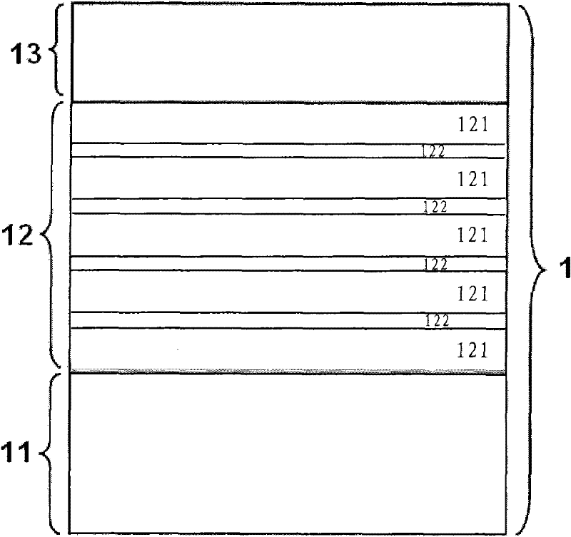
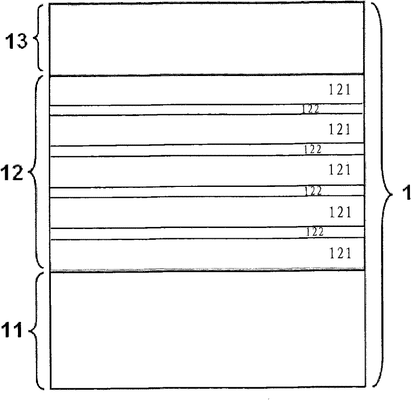
[0034] The technological process for preparing a silicon (Si)-based composite substrate for the preparation of gallium nitride (GaN) LED epitaxial wafer materials by metal-organic chemical vapor deposition (MOCVD) is as follows.

[0035] Step 1: Take a 4-inch Si single crystal substrate 11 with a Si(111) plane;

[0036] Step 2: Put the cleaned Si(111) single crystal substrate 11 into the MOCVD equipment reaction chamber;

[0037] Step 3: Prepare and grow a thin AlN single crystal film material 121 with a thickness of 50 nm on the Si(111) single crystal substrate 11 by MOCVD process as a barrier layer and a lattice mismatch stress covariant layer;

[0038] Step 4: Prepare and grow a 10nm-thick ultra-thin TiN single crystal thin film material 122 on the 50nm-thick AlN layer 121 by MOCVD process as a thermal stress covariant layer.

[0039] Step 5: Repeat steps 3 and 4 to prepare a composite stress-conforming layer material 12 composed of five overlapping 50nm thin AlN layers 12...


PUM

PropertyMeasurementUnit
thicknessaaaaaaaaaa
diameteraaaaaaaaaa

Abstract

The invention provides a silicon-base compound substrate for preparing a nitride semiconductor epitaxial material, and a manufacturing method of the silicon-base compound substrate. The silicon-base compound substrate comprises a silicon monocrystal substrate, a compound stress covariant layer which is formed on the silicon monocrystal substrate and formed by frequently stacking aluminum nitride and a titanium nitride monocrystal thin film material, and a gallium nitride template layer which is formed on the compound stress covariant layer and consists of a gallium nitride monocrystal thin film material. By the silicon-base compound substrate, the crystal lattice and big heat mismatch problems of the silicon-base gallium nitride material are solved; therefore, the preparation cost of a gallium nitride light emitting diode (LED) epitaxial sheet can be reduced greatly; and the silicon-base compound substrate is suitable for application and market popularization.

Description

technical field [0001] The invention relates to a semiconductor substrate and a manufacturing method thereof, in particular to a silicon-based composite substrate for preparing nitride semiconductor epitaxial materials and a manufacturing method thereof. Background technique [0002] Nitride semiconductors, especially gallium nitride (GaN) are the core basic materials for preparing light-emitting diode devices used in the fields of semiconductor lighting and display backlighting. Due to the lack of homogeneous single-crystal materials, device applications of GaN materials are usually carried out on heterogeneous substrates, most commonly sapphire (Al 2 o 3 ) substrate, because the sapphire substrate is non-conductive, hard and expensive, it has been difficult to reduce the difficulty and cost of GaN-based LED devices on it. Compared with sapphire and GaN, silicon carbide (SiC) substrate has a better lattice matching relationship, but it is expensive, and the GaN-based LED ...

Claims


Application Information

Patent Timeline
Patent Type & Authority Applications(China)
IPC IPC(8): H01L21/20H01L33/12
Inventor 施建江杨少延刘祥林
Owner 杭州海鲸光电科技有限公司
Why Eureka
Try Eureka