Method for manufacturing metal laminated substrate for semiconductor element formation and metal laminated substrate for semiconductor element formation

A manufacturing method and semiconductor technology, which are applied in the fields of semiconductor/solid-state device manufacturing, semiconductor/solid-state device components, semiconductor devices, etc., can solve the roughness of the bonding interface, uneven deformation, and difficulty in stably manufacturing highly crystalline substrates, etc. question

Active Publication Date: 2011-10-05
TOYO KOHAN CO LTD
View PDF8 Cites 6 Cited by
  • Summary
  • Abstract
  • Description
  • Claims
  • Application Information

AI Technical Summary

Problems solved by technology

In addition, it is known that in order to highly crystallize the Ni layer after the diffusion heat treatment, a processing rate of 90% or more is required. When performing strong rolling in a state where different types of metals are bonded, due to the mechanical properties of the two materials, difference, and the difference in extension between materials produces larger warpage
Therefore, it is not easy to manufacture wide and long materials
[0013] In addition, in the above-mentioned cladding material, the bonding materials are constrained to each other at the bonding interface, causing uneven deformation and being rolled, so that uniform strain cannot be introduced in the thickness direction.
[0014] In addition, the thickness of the bonding interface is also rough, so the thickness of the crystal-oriented Ni layer also becomes non-uniform, and it is difficult to stably manufacture a substrate having uniform and highly crystalline orientation in the longitudinal direction in the heat treatment after bonding.

Method used


Image

  • Method for manufacturing metal laminated substrate for semiconductor element formation and metal laminated substrate for semiconductor element formation
  • Method for manufacturing metal laminated substrate for semiconductor element formation and metal laminated substrate for semiconductor element formation
  • Method for manufacturing metal laminated substrate for semiconductor element formation and metal laminated substrate for semiconductor element formation

Examples


Embodiment 1

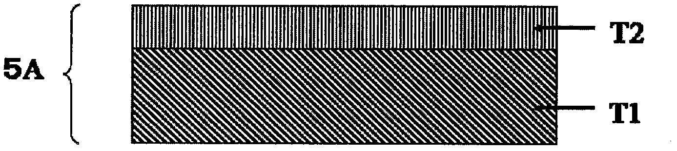
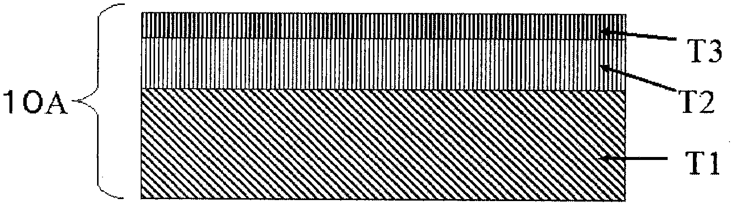
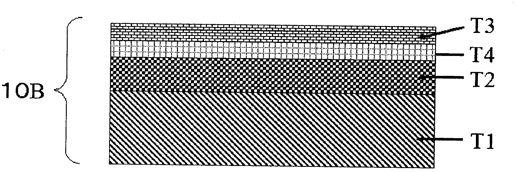
[0094] Hereinafter, examples of the present invention will be disclosed, and properties of the obtained metal laminated substrate will be described. A 200 mm wide, 18 μm thick high pressure rolled Cu foil (metal foil) and a 100 μm thick SUS316L plate (metal plate) were joined by surface activation bonding at room temperature, and then heat-treated at 200°C to 1000°C for 5 minutes. Metal build-up substrates.

[0095] Table 1 shows the ratio of the Cu (200) plane parallel to the Cu foil surface at this time, that is, the crystal orientation ratio (diffraction peak intensity ratio of the (200) plane of the θ / 2θ diffraction peak measured by X-ray diffraction: I (200) / ∑I (hkl) ×100(%)), and means that the (200) plane is parallel to the length direction , that is, ΔΦ° (the Φ scanning peak obtained in the Ni(111) pole diagram obtained by X-ray diffraction as an index of biaxial crystal orientation ( Average value of the half-value widths of the 4 peaks at α=35°)).

[0096] Compar...


PUM

PropertyMeasurementUnit
thicknessaaaaaaaaaa
thicknessaaaaaaaaaa
thicknessaaaaaaaaaa

Abstract

Disclosed is a metal laminated substrate for epitaxially grown film formation for semiconductor element formation, the metal laminated substrate comprising a metal substrate having a high biaxially crystal-aligned surface. Also disclosed is a method for manufacturing the metal laminated substrate, comprising the steps of activating at least one surface of a metal plate (T1) by sputter etching or the like, activating at least one surface of a metal foil (T2) formed of Cu or a Cu alloy which has been cold rolled with a reduction of not less than 90%, stacking the metal plate and the metal foil on top of each other so that the activated surface of the metal plate faces the activated surface of the metal foil, cold rolling the laminate, for example, with a reduction of not more than 10%, and heat treating the cold rolled laminate at 150 to 1000 DEG C for biaxial crystal alignment of the metal foil.

Description

technical field [0001] The present invention relates to a method of manufacturing a metal laminated substrate for forming an epitaxial growth film formed on a semiconductor element, and a metal laminated substrate for forming an epitaxial growth film formed on a semiconductor element. Background technique [0002] In order to obtain an excellent semiconductor device, it is necessary to form an epitaxial growth film with high alignment on a substrate. [0003] Therefore, conventionally, single crystal silicon (Si), single crystal gallium arsenide (GaAs), single crystal sapphire (Al 2 o 3 ) and other single crystal wafers. [0004] However, the size of these single crystal wafers is relatively large and is about 300mmΦ, so it cannot be formed into a film by a continuous production method such as a roll-to-roll method. In addition, Si and the like have no strength, and are not easy to handle during the transfer of the manufacturing steps, so special attention is required. ...

Claims


Application Information

Patent Timeline
Patent Type & Authority Applications(China)
IPC IPC(8): H01L21/20B21B47/00B23K20/00B23K20/24C22F1/08C22F1/00
CPCB32B15/01H01L23/142C30B29/16C30B29/52H05K1/09H05K2201/0355H01L31/03921C22C9/00H01L33/007C22F1/08B32B15/015Y02E10/50H05K1/0393C22C38/44H05K2203/1105C30B29/06C30B29/40C30B33/00C22C38/02C30B25/18H05K3/022C22C38/58H01L2924/0002H01L2924/00B21B47/00H01L21/20
Inventor 冈山浩直金子彰南部光司
Owner TOYO KOHAN CO LTD
Why Eureka
Try Eureka