Germanium-based NMOS (N-metal-oxide-semiconductor) device and preparation method thereof

A germanium-based device technology, applied in the field of germanium-based NMOS device structure and preparation, can solve the problems of large electronic potential barrier, limit the performance of germanium-based Schottky NMOS transistors, etc., achieve low source-drain resistance, suppress Fermi energy Level pinning effect, the effect of reducing the Schottky barrier

Active Publication Date: 2011-10-19
SEMICON MFG INT (BEIJING) CORP +1
View PDF4 Cites 16 Cited by
  • Summary
  • Abstract
  • Description
  • Claims
  • Application Information

AI Technical Summary

Problems solved by technology

However, germanium-based Schottky MOS transistors also have problems to be solved: a large number of interface states make the Fermi level pinned near the valence band, resulting in a large electronic potential barrier, which limits the performance of germanium-based Schottky NMOS transistors. promote

Method used


Image

  • Germanium-based NMOS (N-metal-oxide-semiconductor) device and preparation method thereof
  • Germanium-based NMOS (N-metal-oxide-semiconductor) device and preparation method thereof
  • Germanium-based NMOS (N-metal-oxide-semiconductor) device and preparation method thereof

Examples


Embodiment Construction

[0024] Below in conjunction with accompanying drawing and specific embodiment the present invention is described in further detail:

[0025] FIG. 1 is a flowchart of a method for fabricating a germanium-based Schottky transistor according to a preferred embodiment of the present invention. The method for making germanium-based Schottky transistor of the present invention comprises the following steps:

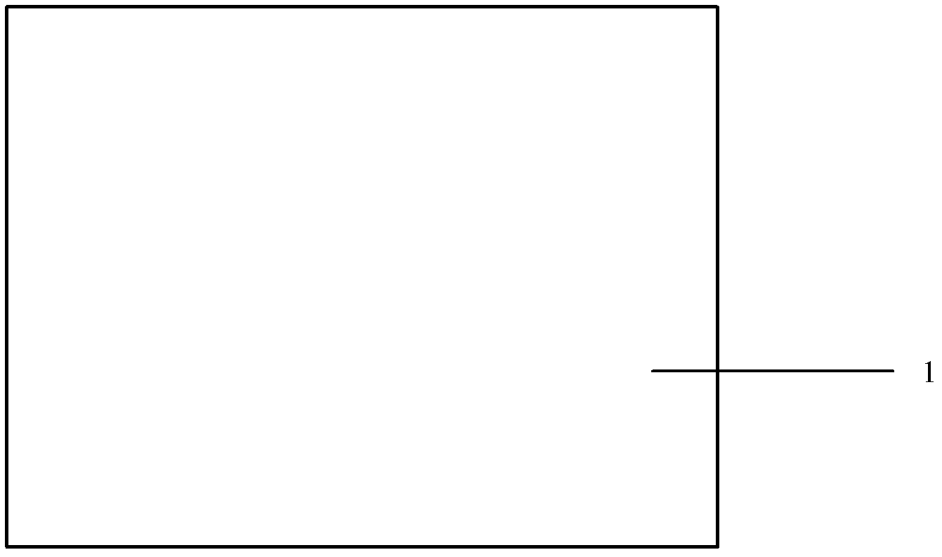
[0026] Step 1: Provide a germanium-based substrate. As shown in FIG. 1(a), an N-type semiconductor germanium substrate 1, wherein the substrate 1 can be bulk germanium, germanium-on-insulator (GOI) or epitaxial germanium substrate.

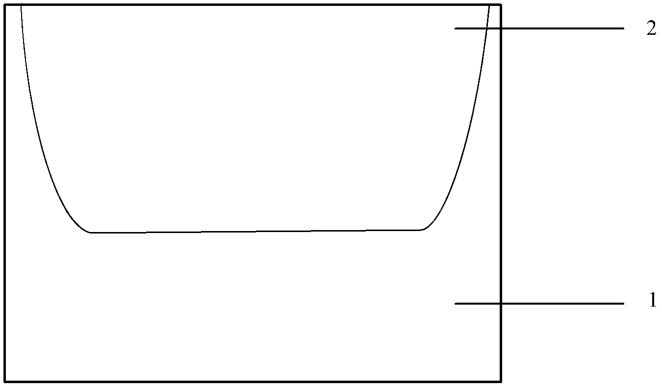
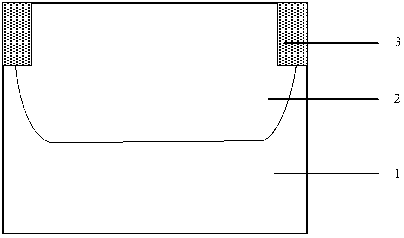
[0027] Step 2: Fabricate the P-well region. Deposit silicon oxide and silicon nitride layers on the germanium substrate, first define the P-well region by photolithography and reactive ion etching away the silicon nitride in the P-well region, then ion implant P-type impurities such as boron, etc., and then anneal to drive Into the production of...


PUM

PropertyMeasurementUnit
thicknessaaaaaaaaaa
thicknessaaaaaaaaaa

Abstract

The invention provides a germanium-based NMOS (N-metal-oxide-semiconductor) device and a preparation method thereof, belonging to the technical field of ultra large scale integration (ULSI) circuit manufacturing. Two layers of insulation medium material are inserted among metal source and drain electrodes and a substrate of the germanium based-NMOS device, and the bottom layer is S medium material with high pinning coefficient, such as hafnium oxide, silicon nitride or hafnium silica, and the upper layer of medium material is delta EC medium material with low conduction band offset, such as titanium dioxide, gallium oxide or strontium titanium oxygen. According to the invention, the fermi energy level pinning effect can be weakened, the electronic potential barrier is reduced, and furtherthe performances of a germanium-based schottky NMOS device are improved; and compared with the traditional method in which a single layer of insulation medium material such as AL2O3 is adopted, the preparation method can be used for effectively reducing the schottky potential barrier and maintaining lower source and drain resistance, therefore, the performances of the device are improved to a large extent.

Description

technical field [0001] The invention belongs to the technical field of ultra-large-scale integrated circuit (ULSI) manufacturing technology, and in particular relates to a germanium-based NMOS device structure and a preparation method thereof. Background technique [0002] As the size of CMOS devices continues to shrink, traditional silicon-based MOS devices have encountered many challenges, among which mobility degradation has become one of the key factors affecting the further improvement of device performance. Compared with silicon materials, germanium materials have higher and more symmetrical low-field carrier mobility, and the preparation process of germanium channel devices is compatible with traditional CMOS processes. Therefore, germanium-based devices have become one of the current research hotspots. [0003] Germanium-based Schottky MOS transistor is a very potential device structure. The main difference between it and the traditional MOS transistor is that the s...

Claims


Application Information

Patent Timeline
Patent Type & Authority Applications(China)
IPC IPC(8): H01L29/47H01L29/78H01L29/06H01L21/28H01L21/336
CPCH01L29/78H01L29/41783H01L29/517H01L29/66643H01L29/0895
Inventor 黄如李志强安霞郭岳张兴
Owner SEMICON MFG INT (BEIJING) CORP
Why Eureka
Try Eureka