Preparation method of high temperature superconductive coating conductor buffer layer
A technology of coated conductors and high-temperature superconductors, applied in cable/conductor manufacturing, electrical components, circuits, etc., can solve problems such as slow preparation speed, difficulty in long tapes, and complicated equipment, and achieve low equipment cost and small surface roughness , the effect of good c-axis texture
- Summary
- Abstract
- Description
- Claims
- Application Information
AI Technical Summary
Problems solved by technology
Method used
Image
Examples
Embodiment 1
[0035] (1) Nd(acac) 3 2H 2 O and Zr(acac) 4 Mix by a molar ratio of 1:1, then add an organic solvent to the mixture to prepare a precursor solution with a molar concentration of cations of 0.4mol / L; the organic solvent is a mixed solvent of propionic acid and methanol, and in the mixed solvent propionic acid and methanol The volume ratio is 3:2;
[0036] (2) Add 50 μL of the precursor solution described in step (1) dropwise on the ultrasonically cleaned YSZ single crystal substrate (10mm×10mm), and spin coat it with a spin coater at a rotation rate of 2500 rpm for 30s. Apply the precursor solution evenly on the substrate, and then dry it at a temperature not higher than 200°C;
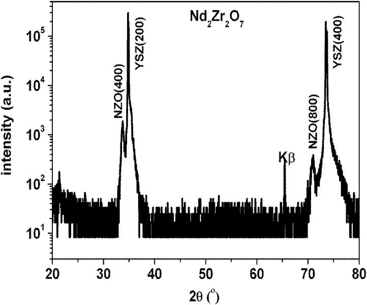
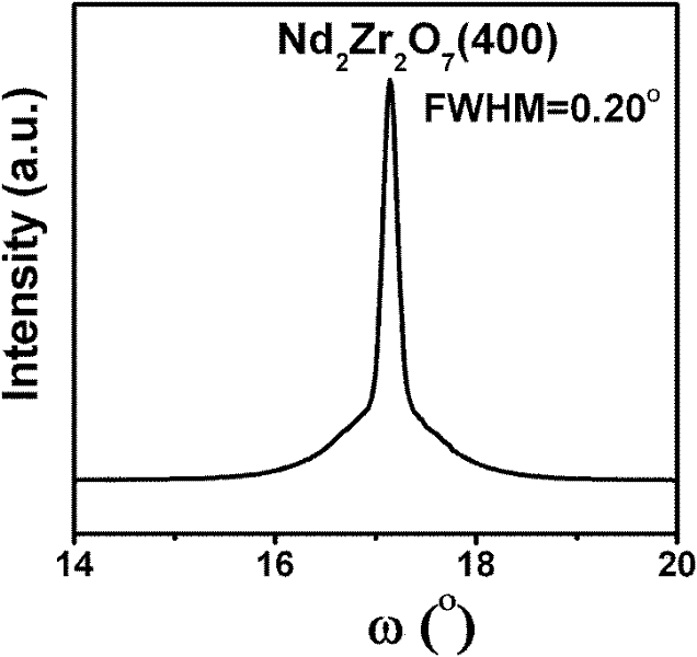
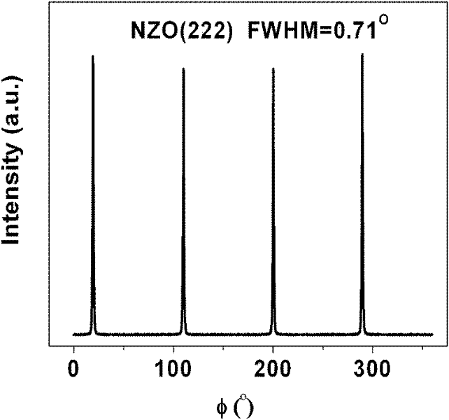
[0037] (3) The YSZ single crystal substrate after drying in the step (2) is placed in the tube furnace, and the gas flow rate is 48L / h Ar-4%H 2 Under the atmosphere, heat up to 500°C at a heating rate of 25°C / min and then hold for 1 hour, then continue to heat up to 1000°C at a heating rate of 25°C...
Embodiment 2
[0041] The preparation method of this embodiment is the same as that of Example 1, wherein the difference is that the raw material used is Sm(acac) 3 ·H 2 O, prepared Sm with good c-axis texture and small surface roughness (RMS less than 5nm) 2 Zr 2 o 7 The buffer layer.
[0042] Sm prepared in this example 2 Zr 2 o 7 The X-ray diffraction pattern of the buffer layer is as Figure 5 , Sm 2 Zr 2 o 7 The ω-scan spectrum of the buffer layer is as follows Figure 6 , Sm 2 Zr 2 o 7 The Φ scan pattern of the buffer layer is as follows Figure 7 , Sm 2 Zr 2 o 7 The atomic force microscope (AFM) photograph of the buffer layer is as Figure 8 .
[0043] From Figure 5 It can be seen that, except for the (200), (400) diffraction peaks of the YSZ single crystal substrate and the K β Outside the peak, only Sm 2 Zr 2 o 7 The (400) and (800) diffraction peaks of the film indicate that only a single Sm 2 Zr 2 o 7 phase with a c-axis orientation. From Figure 6 an...
Embodiment 3
[0045] (1) Nd(acac) 3 2H 2 O and Zr(acac) 4 Mix by a molar ratio of 1:1, then add an organic solvent to the mixture to prepare a precursor solution with a molar concentration of cations of 0.4mol / L; the organic solvent is a mixed solvent of propionic acid and methanol, and in the mixed solvent propionic acid and methanol The volume ratio is 3:2;
[0046] (2) Add 50 μL of the precursor solution described in step (1) dropwise on the Ni-W alloy substrate (10mm×10mm) after ultrasonic cleaning, and spin-coat at a spin rate of 2500 rpm for 30s with a coater , so that the precursor solution is evenly coated on the substrate, and then dried at a temperature not higher than 200°C;
[0047] (3) Place the Ni-W alloy substrate after drying in the step (2) in the tube furnace, and in the Ar-4%H that the gas flow rate is 48L / h 2 Under the atmosphere, heat up to 300°C at a heating rate of 25°C / min and then hold for 1 hour, then continue to heat up to 1000°C at a heating rate of 25°C / min ...
PUM
| Property | Measurement | Unit |
|---|---|---|
| surface roughness | aaaaa | aaaaa |
| surface roughness | aaaaa | aaaaa |
Abstract
Description
Claims
Application Information


