
Excessive-plating prevention dual-layer thin film as well as preparation method and application thereof

A double-layer film and thin-layer technology, applied in the field of solar energy, can solve problems such as corrosion, overplating, and disappearance of double-layer anti-reflection film characteristics, so as to improve product yield and stability, simplify the preparation process, and improve needle hole effect

Inactive Publication Date: 2011-11-16
INST OF ELECTRICAL ENG CHINESE ACAD OF SCI +1
View PDF8 Cites 8 Cited by
  • Summary
  • Abstract
  • Description
  • Claims
  • Application Information

AI Technical Summary

Problems solved by technology

In these structures, the fundamental purpose is to realize the function of the double-layer anti-reflection film, and does not involve the content of preventing solar cells from overplating; It is etched by HF solution or other solutions containing F ions, which will cause the oxide layer to be corroded quickly or expose defects in the film: pinholes, cracks, etc., so it cannot meet the needs of those who need HF before preparing electrodes. Solution or other etching process requirements containing F ion solution can not achieve the purpose of preventing overplating, and at the same time the characteristics of its double-layer anti-reflection film will also disappear.
Many conventional masking methods or methods of processing silicon nitride films are not suitable, especially where HF or F ion etching is required on the front surface of the solar cell prior to metal deposition
However, there is no suitable method for the treatment of the battery after forming the overplating so that it can meet the requirements of commercialization.

Method used


Image

  • Excessive-plating prevention dual-layer thin film as well as preparation method and application thereof
  • Excessive-plating prevention dual-layer thin film as well as preparation method and application thereof
  • Excessive-plating prevention dual-layer thin film as well as preparation method and application thereof

Examples


preparation example Construction

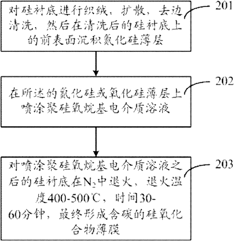
[0028] figure 2 Shown is the flow chart of the preparation method embodiment of double-layer thin film of the present invention, and it comprises the following steps:

[0029] Step 201, performing weaving, diffusion, edge cleaning on the silicon substrate, and then depositing a silicon nitride thin layer on the front surface of the cleaned silicon substrate;

[0030] Step 202, spraying polysiloxane-based dielectric solution on the silicon nitride or silicon oxide thin layer;

[0031] Step 203, spraying the silicon substrate after the polysiloxane-based dielectric solution on N 2 Medium annealing, the annealing temperature is 400-500° C., and the time is 30-60 minutes, finally forming a carbon-containing silicon oxide film.

[0032] Before step 203 is performed, the silicon substrate may be placed on a hot plate and dried at a temperature of 200° C. for 30 seconds.

[0033] In the present invention, a thin layer of silicon oxide may also be deposited on the surface of the s...

Embodiment 1

[0039] 1. The silicon substrate is processed according to the conventional production line process: P-type polysilicon is used, the surface of the silicon substrate is woven with acidic solution, POCl 3 The liquid source is diffused to form a PN junction, edge cleaning is performed, silicon nitride is deposited by PECVD, and Ag and Al electrodes are screen-printed on the back.

[0040] 2. Deposit hydrophobic dielectric film by spraying method: configure IC1-200 and isopropanol according to the volume ratio of 1:1 to form a diluted IC1-200 solution, and then use 10ml / min on the spraying equipment PV-360 The spraying speed is sprayed once, and the spraying speed determines the thickness of the film, and the thickness of the film obtained at this speed is 25nm.

[0041] 3. Place the silicon substrate sprayed with IC1-200 on a hot plate, and dry it in the air at 200°C for 30 seconds to remove isopropanol and other organic components in the film.

[0042] 4. In the air, place the ...

Embodiment 2

[0044] 1. The silicon substrate is processed according to the conventional production line process: P-type polysilicon is used, the surface of the silicon substrate is woven with acidic solution, POCl 3 The liquid source is diffused to form a PN junction, edge cleaning is performed, silicon nitride is deposited by PECVD, and Ag and Al electrodes are screen-printed on the back.

[0045] 2. Deposit hydrophobic dielectric film by spraying method: configure IC1-200 and isopropanol at a volume ratio of 1:1 to form a diluted IC1-200 solution, and then spray it on PV-360 at a rate of 20ml / min Spraying was carried out at a spraying speed, spraying twice, and the thickness of the obtained film was 100 nm.

[0046] 3. Place the silicon substrate sprayed with IC1-200 on a hot plate, and dry it in air at 200°C for 30 seconds to remove isopropanol and other organic components in the film.

[0047] 4. In the air, place the silicon substrate prepared in step 3 on a hot plate and anneal at 4...


PUM

PropertyMeasurementUnit
Thicknessaaaaaaaaaa
Thicknessaaaaaaaaaa
Thicknessaaaaaaaaaa

Abstract

The invention discloses an excessive-plating prevention dual-layer thin film which is characterized in that: one layer adjacent to the front surface of a silicon substrate is a silicon oxide or silicon nitride thin layer; and a layer above the silicon oxide or silicon nitride thin layer is a carbon-containing silicon-oxygen compound thin layer, wherein the carbon atom content in the carbon-containing silicon-oxygen compound thin layer is 5-10%, the refraction coefficient is 1.3-1.4, and the thickness is 20-200 nm. A preparation method of the dual-layer thin film comprises the following steps:depositing a silicon oxide or silicon nitride thin layer on the front surface of the cleaned silicon substrate; spraying or spinning a polysiloxane-based dielectric solution on the thin layer; and annealing to obtain the dual-layer thin film. A silicon solar cell comprising the dual-layer thin film is sequentially provided with a dual-layer thin film, a front electrode, an n<+> emitter, a p-type silicon area, a local back electric field p<+> and a back electrode downward from a sunlight irradiation surface, namely the front surface.

Description

technical field [0001] The invention relates to the technical field of solar energy, in particular to a thin film preventing overplating, a preparation method thereof and an applied silicon solar cell. Background technique [0002] "Overplating" means electroplating metal where it is not desired to be present. For solar cells that require selective plating, overplating has a great influence on their performance. On the one hand, depositing metal on other non-metal deposition areas will lead to an increase in metal shading, thereby reducing the amount of light entering the solar cell; on the other hand, overplating will lead to electrical short circuits and other problems. Overplating can also lead to waste of electroplating materials, especially for electroplating substances that are some special materials, such as precious metals Ag, Au, etc., resulting in an increase in the production cost of solar cells. [0003] Many conventional selective platings require multiple ste...

Claims


Application Information

Patent Timeline
IPC IPC(8): H01L31/18C23C28/04
CPCY02P70/50
Inventor 周春兰王文静李涛宋洋李友忠段野郜志华
Owner INST OF ELECTRICAL ENG CHINESE ACAD OF SCI
Learn More