

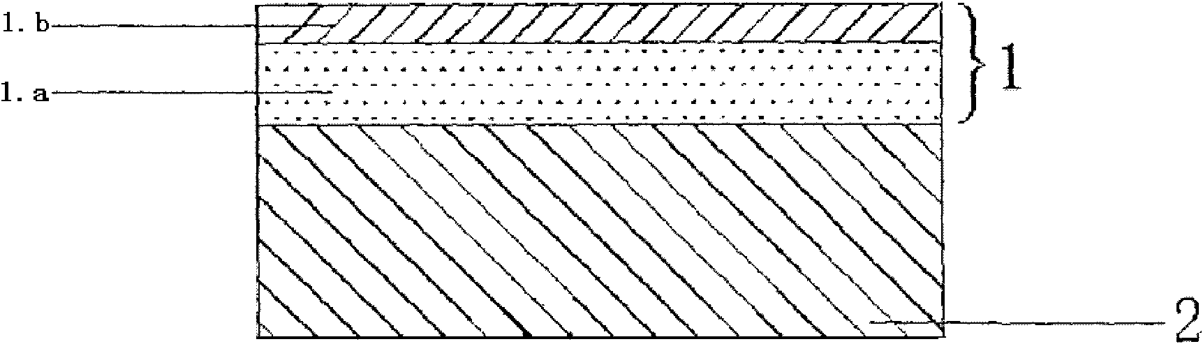
Excessive-plating prevention dual-layer thin film as well as preparation method and application thereof
A double-layer film and thin-layer technology, applied in the field of solar energy, can solve problems such as corrosion, inability to overcoat, and disappearance of double-layer anti-reflection film characteristics, so as to improve product yield and stability, simplify the preparation process, and prevent overcoating. The effect of plating
- Summary
- Abstract
- Description
- Claims
- Application Information
AI Technical Summary
Problems solved by technology
Method used
Image

Examples
preparation example Construction
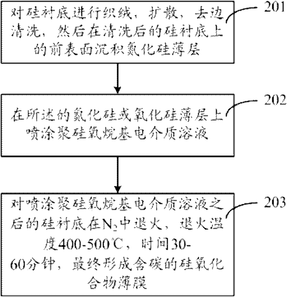
[0028] figure 2 Shown is the flow chart of the preparation method embodiment of double-layer thin film of the present invention, and it comprises the following steps:
[0029] Step 201, performing weaving, diffusion, edge cleaning on the silicon substrate, and then depositing a silicon nitride thin layer on the front surface of the cleaned silicon substrate;
[0030] Step 202, spraying polysiloxane-based dielectric solution on the silicon nitride or silicon oxide thin layer;
[0031] Step 203, spraying the silicon substrate after the polysiloxane-based dielectric solution on N 2 Medium annealing, the annealing temperature is 400-500° C., and the time is 30-60 minutes, finally forming a carbon-containing silicon oxide film.
[0032] Before step 203 is performed, the silicon substrate may be placed on a hot plate and dried at a temperature of 200° C. for 30 seconds.
[0033] In the present invention, a thin layer of silicon oxide may also be deposited on the surface of the s...
Embodiment 1
[0039] 1. The silicon substrate is processed according to the conventional production line process: P-type polysilicon is used, the surface of the silicon substrate is woven with acidic solution, POCl 3 The liquid source is diffused to form a PN junction, edge cleaning is performed, silicon nitride is deposited by PECVD, and Ag and Al electrodes are screen-printed on the back.
[0040] 2. Deposit hydrophobic dielectric film by spraying method: configure IC1-200 and isopropanol according to the volume ratio of 1:1 to form a diluted IC1-200 solution, and then use 10ml / min on the spraying equipment PV-360 The spraying speed is sprayed once, and the spraying speed determines the thickness of the film, and the thickness of the film obtained at this speed is 25nm.
[0041] 3. Place the silicon substrate sprayed with IC1-200 on a hot plate, and dry it in the air at 200°C for 30 seconds to remove isopropanol and other organic components in the film.
[0042] 4. In the air, place the ...
Embodiment 2
[0044] 1. The silicon substrate is processed according to the conventional production line process: P-type polysilicon is used, the surface of the silicon substrate is woven with acidic solution, POCl 3 The liquid source is diffused to form a PN junction, edge cleaning is performed, silicon nitride is deposited by PECVD, and Ag and Al electrodes are screen-printed on the back.
[0045] 2. Deposit hydrophobic dielectric film by spraying method: configure IC1-200 and isopropanol at a volume ratio of 1:1 to form a diluted IC1-200 solution, and then spray it on PV-360 at a rate of 20ml / min Spraying was carried out at a spraying speed, spraying twice, and the thickness of the obtained film was 100 nm.
[0046] 3. Place the silicon substrate sprayed with IC1-200 on a hot plate, and dry it in air at 200°C for 30 seconds to remove isopropanol and other organic components in the film.
[0047] 4. In the air, place the silicon substrate prepared in step 3 on a hot plate and anneal at 4...
PUM
| Property | Measurement | Unit |
|---|---|---|
| thickness | aaaaa | aaaaa |
| thickness | aaaaa | aaaaa |
| thickness | aaaaa | aaaaa |
Abstract
Description
Claims
Application Information