

Rectangular micro heating device with heating resistance wire with non-uniform wire width and heating method
A technology for heating resistance wires and heaters, applied in ohmic resistance heating parts, microstructure technology, microstructure devices, etc., can solve the problems of increasing heater power consumption, affecting mechanical strength, and complex process, etc., to reduce heat conduction , The manufacturing process is simple, the effect of uniform temperature distribution
- Summary
- Abstract
- Description
- Claims
- Application Information
AI Technical Summary
Problems solved by technology
Method used
Image

Examples
Embodiment 1
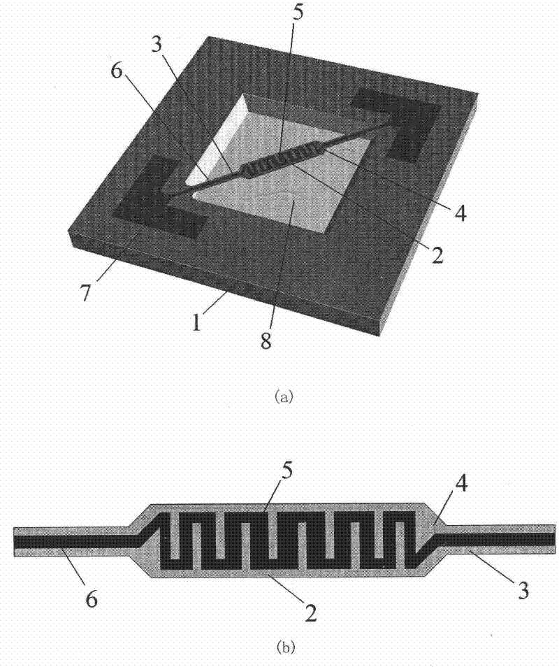
[0035] The structure schematic diagram of this embodiment sees figure 1 As shown in (a), the specific production method is as follows:
[0036] 1. Select the substrate. A 4-inch double-sided polished silicon wafer with an N-type (100) surface is selected as a substrate, the resistivity is 3-8Ω·cm, the thickness of the silicon wafer is 350±10 microns, and the angle error of trimming is <1%.
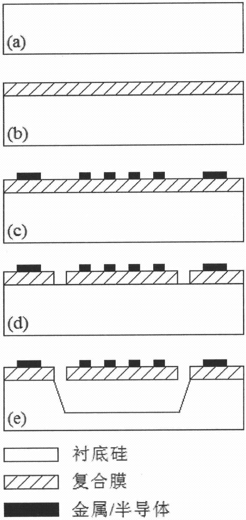
[0037]2. Make a composite film. A single-layer composite film is used to sequentially grow a layer of silicon oxide with a thickness of 0.5 microns and a layer of silicon nitride with a thickness of 0.3 microns by means of low-pressure chemical vapor deposition (LPCVD).
[0038] 3. Make zigzagging heating resistance wires, leads and electrodes. Manufactured using a lift-off process. Thin-resist lithography (photoresist thickness is 2.0 microns) defines the pattern of zigzag heating resistance wires, leads and electrodes, then sputters a layer of 0.2-micron thick titanium platinum, and ...
Embodiment 3
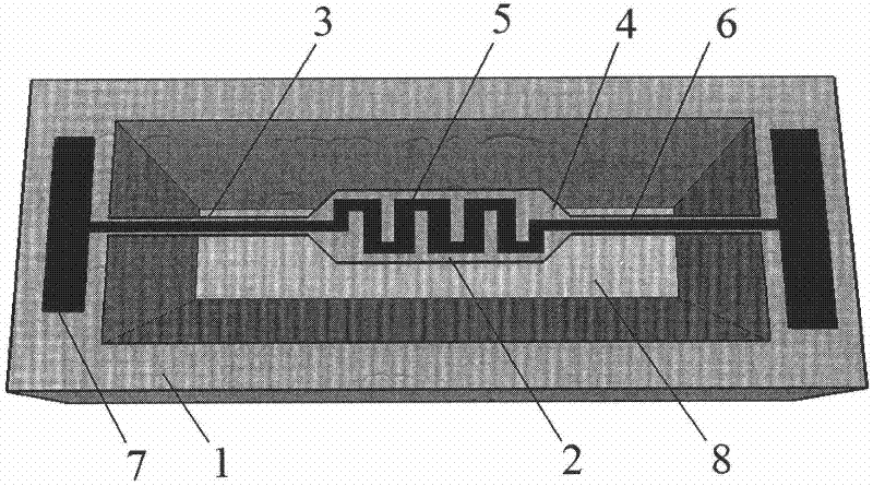
[0049] The structure schematic diagram of this embodiment sees Figure 4 As shown, the specific production method is as follows:
[0050] 1. Substrate selection. A 4-inch double-sided polished silicon wafer with a P-type (100) surface is selected as the substrate, the resistivity is 3-8Ω·cm, the thickness of the silicon wafer is 350±10 microns, and the angle error of the edge trimming is less than 1%.
[0051] 2. Make a composite film. Using a multi-layer composite film, a layer of silicon oxide with a thickness of 0.2 microns and a layer of silicon nitride with a thickness of 0.2 microns are sequentially deposited by low-pressure chemical vapor deposition (LPCVD), and then plasma-enhanced chemical vapor deposition (PECVD) A method of depositing a layer of silicon oxide with a thickness of 0.2 microns and a layer of silicon nitride with a thickness of 0.2 microns in sequence.
[0052] 3. Make zigzagging heating resistance wires, leads and electrodes. Manufactured by lift-o...
PUM
| Property | Measurement | Unit |
|---|---|---|
| Resistivity | aaaaa | aaaaa |
| Thickness | aaaaa | aaaaa |
Abstract
Description
Claims
Application Information