Preparation method of silicon-based gallium arsenide material structure applied to nmos

A silicon-based gallium arsenide, material structure technology, used in semiconductor/solid-state device manufacturing, electrical components, circuits, etc., can solve problems such as inability to extend, and achieve the effects of improving quality, reducing defects, and optimizing growth rate

Active Publication Date: 2011-11-30
INST OF SEMICONDUCTORS - CHINESE ACAD OF SCI
View PDF3 Cites 14 Cited by
  • Summary
  • Abstract
  • Description
  • Claims
  • Application Information

AI Technical Summary

Problems solved by technology

Thus, when these misfit dislocations and APDs encounter SiO 2 wall is blocked from extending to the top layer of GaAs

Method used


Image

  • Preparation method of silicon-based gallium arsenide material structure applied to nmos
  • Preparation method of silicon-based gallium arsenide material structure applied to nmos
  • Preparation method of silicon-based gallium arsenide material structure applied to nmos

Examples


Embodiment Construction

[0030] see Figure 1 to Figure 6 , the present invention provides a method for preparing a silicon-based gallium arsenide material structure applied to nMOS, comprising the following steps:

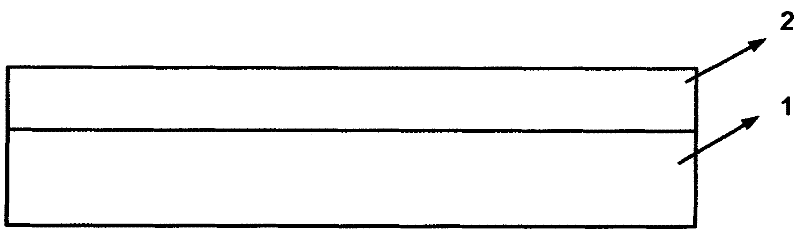
[0031] Step 1: growing a silicon dioxide layer 2 on a silicon substrate 1, the silicon substrate 1 is high-resistance (001) silicon with a p-type resistivity greater than 2000Ωcm, and the thickness of the silicon dioxide layer 2 is 500nm-1000nm ;

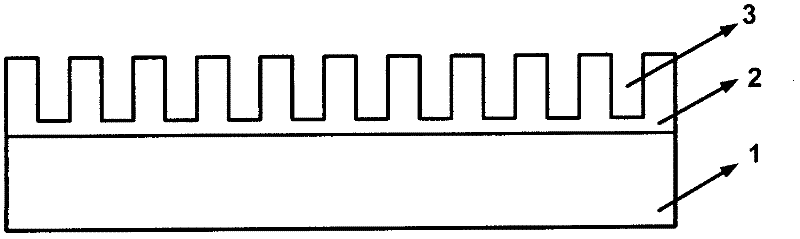
[0032] Step 2: using traditional photolithography and RIE methods to etch a plurality of trenches 3 on the silicon dioxide layer 2 along the direction of the silicon substrate 1, and the width of the trenches 3 is 200-300nm;

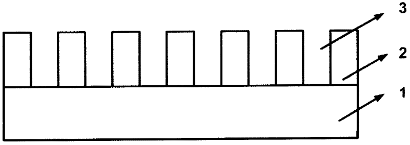
[0033] Step 3: Use piranha and SC respectively 2 , HF and deionized water cleaning, remove the remaining silicon dioxide layer 2 at the bottom of the trench 3, and expose the silicon substrate 1, the remaining silicon dioxide layer 2 in the trench is to protect the silicon substrate from being damaged by etching ;

...


PUM

PropertyMeasurementUnit
thicknessaaaaaaaaaa

Abstract

The invention discloses a method for preparing a silica-based gallium arsenide material structure applied to an n-channel metal oxide semiconductor (nMOS). The method comprises the following steps of: 1, growing a silicon dioxide layer on a silicon substrate 1; 2, etching a plurality of trenches along the <110> direction of the silicon substrate on the silicon dioxide layer by adopting conventional photoetching and aspect ratio trapping (RIE) methods; 3, washing the trenches by using piranha, SC2, hydrogen fluoride (HF) and de-ionized water to remove residual silicon dioxide layer at the bottom of each trench and expose the silicon substrate; 4, growing gallium arsenide (GaAs) buffer layers in the trenches by adopting a low voltage metal organic chemical vapor deposition (MOCVD) method, and growing GaAs top layers on the GaAs buffer layers in the trenches; and 5, polishing the parts, above the trenches, of the GaAs top layers to make the GaAs top layers flush with the silicon dioxide layer to finish preparing the material structure by adopting a chemical mechanical polishing method.

Description

technical field [0001] The invention relates to a preparation method of combining MOCVD and high aspect ratio trench confinement technology (Aspect Ratio Trapping, ART) to grow silicon-based gallium arsenide material structure applied to nMOS. Background technique [0002] As the core and foundation of the information industry, integrated circuit (IC) technology is not only the driving force for national economic growth and industrial structure upgrading, but also has an irreplaceable strategic position in modern national defense and future wars. In the past forty years, the integrated circuit technology based on silicon CMOS technology has followed Moore's law to increase the working speed of the chip, increase the integration level and reduce the cost by reducing the feature size of the device. The feature size of the integrated circuit is changed from micron scale Evolved to the nanometer scale, it has achieved huge economic benefits and significant progress in science an...

Claims


Application Information

Patent Timeline
Patent Type & Authority Applications(China)
IPC IPC(8): H01L21/205H01L21/18
Inventor 周旭亮于红艳王宝军潘教青王圩
Owner INST OF SEMICONDUCTORS - CHINESE ACAD OF SCI
Why Eureka
Try Eureka