Internally modified substrate for epitaxial growth, crystal film-forming body, device, bulk substrate manufactured using same, and method for manufacturing them

A technology of epitaxial growth and manufacturing methods, applied in chemical instruments and methods, crystal growth, single crystal growth, etc., can solve problems such as the quality of nitride semiconductor films or the uniformity of light-emitting wavelengths, and achieve the goal of improving quality or yield Effect

Active Publication Date: 2011-12-07
NAMIKI PRECISION JEWEL CO LTD +1
View PDF6 Cites 13 Cited by
  • Summary
  • Abstract
  • Description
  • Claims
  • Application Information

AI Technical Summary

Problems solved by technology

[0008] As described above, it can be seen that the warpage of the sapphire substrate greatly changes through a series of ...

Method used


Image

  • Internally modified substrate for epitaxial growth, crystal film-forming body, device, bulk substrate manufactured using same, and method for manufacturing them
  • Internally modified substrate for epitaxial growth, crystal film-forming body, device, bulk substrate manufactured using same, and method for manufacturing them
  • Internally modified substrate for epitaxial growth, crystal film-forming body, device, bulk substrate manufactured using same, and method for manufacturing them

Examples


Embodiment 1

[0170] As the sapphire substrate for forming the modified region pattern, a 2-inch sapphire substrate whose one side was ground was used. The substrate thickness was 430 μm. The warpage shape and warpage amount of the substrate before the modified region pattern is formed are measured by a laser interferometer.

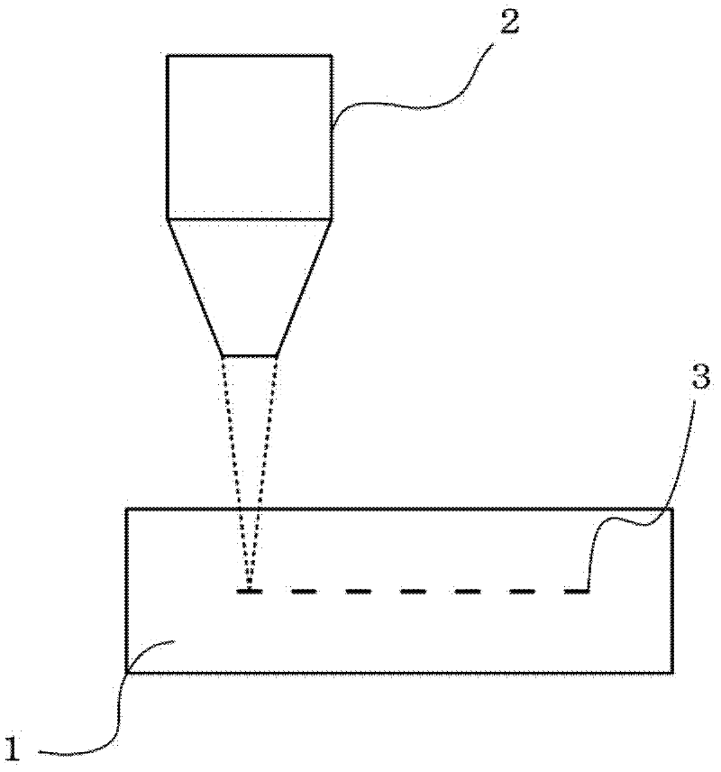
[0171] Next, the sapphire substrate was placed on the sample stage of the pulsed laser device, and the pattern of the modified region inside the sapphire substrate was formed.

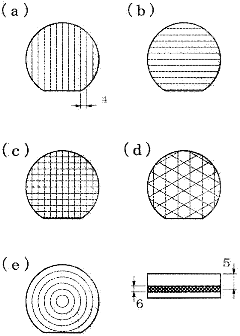
[0172] Table 3 shows the pattern shapes of samples 1 to 9, the distance between each line, the formation position, the length of the modified layer, and the processing time for each sheet. The substrate shape of the sapphire substrate after the modified area pattern is formed is measured by a laser interferometer, and the warpage and substrate thickness are measured by a linear gauge and a laser interferometer. In Table 3, ⊥O.F. means perpendicular to the orientation plane of the sapphire su...

Embodiment 2

[0179] As the sapphire substrate for forming the internal modified region pattern, a 4-inch sapphire substrate whose one side was ground was used. The substrate thickness was 650 μm. Similar to Example 1, the warped shape and warped amount of the substrate before the modified region pattern was formed were measured with a laser interferometer.

[0180]Next, the sapphire substrate was placed on the sample stage of the pulsed laser device, and the pattern of the modified region inside the sapphire substrate was formed. Table 5 shows the pattern shapes, pitches, and formation positions of samples 10 to 19.

[0181] [table 5]

[0182]

[0183] The warped shape of the substrate after the modified region pattern is formed is measured by a laser interferometer, and the warped amount is measured by a linear measuring instrument. Table 6 compares the substrate shape, warpage amount, and curvature calculated from the warpage amount before and after the modified region pattern is f...

Embodiment 3

[0188] Samples 10, 12, 14, 16, and 18 in the sapphire substrate on which the modified region pattern was formed in Example 2, and the existing sapphire substrate (as sample 20) without a pattern were simultaneously introduced into the MOCVD device , and the growth of the GaN layer on the sapphire substrate was carried out. Table 7 shows the growth temperature and film thickness in each film formation process.

[0189] [Table 7]

[0190] Growth temperature (℃)

Film thickness (nm)

AlGaN buffer layer

550

500

n-GaN layer

1070

5000

GaN / InGaN active layer

750

100 / 2

[0191] The In-situ (in-situ) observation results of each sample are shown in Figure 8a ~ Figure 8f In Table 8, the warped shape, warped amount, and curvature of the substrate of each sample are shown in Table 8, and the amount of change in substrate curvature in each step is shown in Table 9.

[0192] (1)~(4) in Table 9, such as Figure ...


PUM

PropertyMeasurementUnit
Thicknessaaaaaaaaaa
Thicknessaaaaaaaaaa

Abstract

Provided is a sapphire substrate mainly for epitaxial growth of a nitride semiconductor layer, wherein the shape and/or the amount of deflection of the substrate can be efficiently and accurately controlled; and the deflection of the substrate occurring when a film is formed is suppressed so that the deflection behavior of the substrate can be reduced. Further, a film forming element for a nitride semiconductor layer, a nitride semiconductor device, and a nitride semiconductor bulk substrate, which are produced using the sapphire substrate, and a method for producing the same are provided. Pulse lasers are concentrated in the inside of the sapphire substrate through the polished surface of the sapphire substrate, to scan the inside of the sapphire substrate, and reforming region patterns are formed using multiphoton absorption performed by the pulse lasers, so that the shape and/or the amount of deflection of the substrate can be controlled. When a nitride semiconductor layer is formed using the sapphire substrate, the deflection of the substrate occurring when a film is formed can be suppressed, and the deflection behavior of the substrate can be reduced. Thus, the quality and the uniformity of the film can be improved, and the quality and the yield ratio of the nitride semiconductor device can be improved.

Description

technical field [0001] The present invention relates to an internally modified substrate for epitaxial growth, a crystal film-formed body, a device, a bulk substrate and their manufacturing method. Background technique [0002] Nitride semiconductors represented by gallium nitride are widely used in LEDs (Light Emitting Diodes) and LDs (Semiconductor Lasers) due to their wide bandgap and ability to emit blue light. In recent years, studies on further improvement of luminous efficiency and higher luminance have been widely carried out. [0003] A general nitride semiconductor light-emitting element structure has a buffer layer composed of GaN, an n-type contact layer composed of n-type GaN, an n-type cladding layer composed of n-type AlGaN, and an n-type cladding layer composed of n-type AlGaN on a sapphire substrate. A double heterostructure consisting of an active layer made of p-type InGaN, a p-type cladding layer made of p-type AlGaN, and a p-type contact layer made of p...

Claims


Application Information

Patent Timeline
IPC IPC(8): H01L21/20B23K26/00C23C16/02C30B29/38C30B33/00H01L21/205C30B25/18
CPCH01L21/0254C30B33/04H01L21/02686H01L21/02458C30B25/186C30B29/403H01L21/0242C30B29/20H01L21/02293
Inventor 会田英雄青田奈津子星野仁志
Owner NAMIKI PRECISION JEWEL CO LTD
Why Eureka
Try Eureka