Buried Mask Wet Etching Process of Silicon Micromechanical Structure

A technology of wet etching and silicon micromechanics, applied in the direction of microstructure technology, microstructure devices, manufacturing microstructure devices, etc., can solve the problems of inability to complete the precise transfer of graphics, easy to damage the film structure, and affect the accuracy of lithography, etc., to achieve Avoid the effects of inaccurate transfer, low process equipment requirements, and product cost reduction

Active Publication Date: 2011-12-14
NAT UNIV OF DEFENSE TECH
View PDF4 Cites 7 Cited by
  • Summary
  • Abstract
  • Description
  • Claims
  • Application Information

AI Technical Summary

Problems solved by technology

[0004] However, there are some problems in the actual operation process, for example: (1) if figure 1 As shown, after a period of corrosion of the silicon wafer, many grooves have been formed on the surface of the silicon wafer. The uniformity of coating on this surface by spin coating is very poor, which cannot meet the requirements of photolithography and cannot complete the precise transfer of graphics. , spraying can apply glue on the uneven surface, but the spraying equipment is expensive, and the thickness uniformity of the sprayed glue layer is not as good as that of the spin-coated glue layer, which affects the lithography accuracy; (2) such as figure 2 As shown, when the surface of the silicon wafer has been corroded to form some very thin film structures, and then the silicon wafer is coated with glue and photolithography, the vacuum suction sheet can easily destroy these film structures, thereby damaging the device. The dotted line in the figure is the suction The shape of the thin film structure when it is deformed after the film

Method used


Image

  • Buried Mask Wet Etching Process of Silicon Micromechanical Structure
  • Buried Mask Wet Etching Process of Silicon Micromechanical Structure
  • Buried Mask Wet Etching Process of Silicon Micromechanical Structure

Examples


Embodiment 1

[0055] Such as Figure 5 ~ Figure 14 Shown, utilize the pre-buried mask wet etching process of silicon micromechanical structure of the present invention, prepare a kind of micro-hot plate that is used in micro-environment, specifically comprise the following steps:

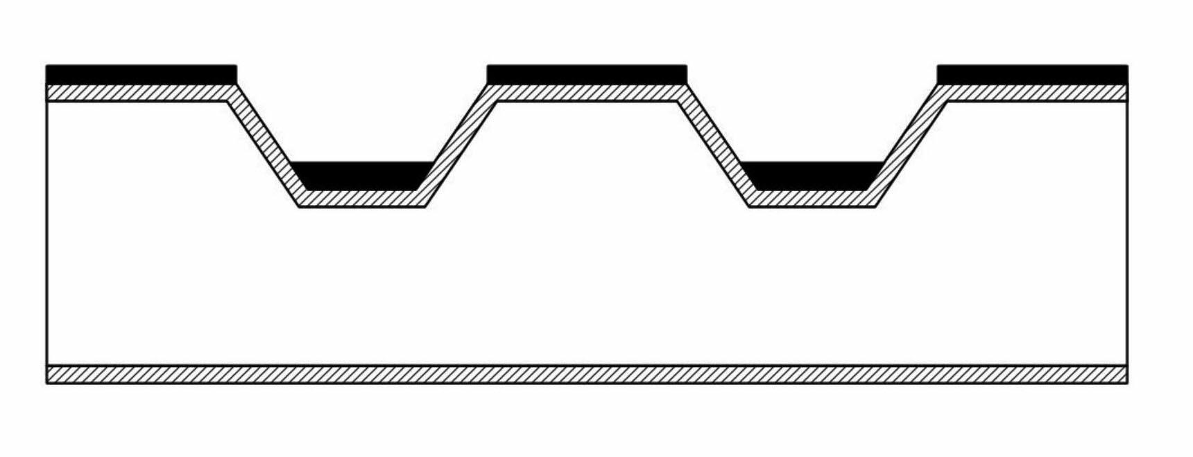
[0056] (1) Preparation of SiO 2 Film layer: such as Figure 5 As shown in the figure, a (100) silicon wafer with N-type double-sided polishing, a resistivity of 0.08Ω·cm to 0.15Ω·cm, and a thickness of 600 μm is selected as the substrate 1 of the silicon micromechanical structure. In a thermal oxidation furnace, thermal oxidation The process produces a thickness of D on the front and back of the silicon wafer 0 =7000 ? of SiO 2 film layer 2;

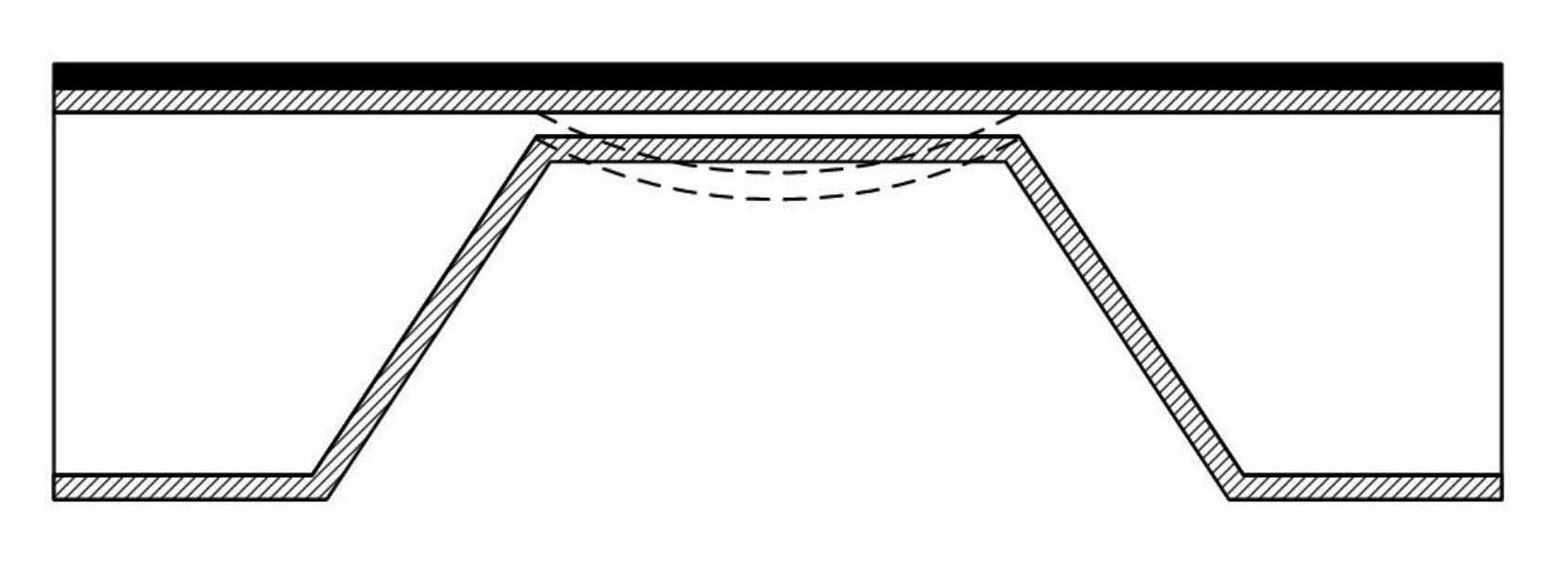
[0057] (2) Prepare mask pattern: such as Figure 6 As shown, the photoresist is evenly spin-coated on the back of the silicon wafer (the photoresist is a positive photoresist, and the spin-coating speed is adjusted to 3500r / min), and the back of the silicon wafer is fi...

Embodiment 2

[0063] Utilize the pre-buried mask wet etching process of the silicon micromechanical structure of the present invention to prepare a single cantilever beam-mass micromechanical structure, such as Figure 17 ~ Figure 26 shown, including the following steps:

[0064] (1) Preparation of SiO 2 Film layer: such as Figure 17 and 18 As shown in Fig. 1, a (100) silicon wafer with N-type double-sided polishing, a resistivity of 0.08Ω·cm-0.15Ω·cm, and a thickness of 200 μm is selected as the substrate 1 of the silicon micromechanical structure. In a thermal oxidation furnace, the silicon wafer is The thermal oxidation process is carried out on the surface, and a thickness of D is formed on the front and back sides of the silicon wafer. 0 =7000 ? of SiO 2 film layer 2;

[0065] (2) Prepare mask pattern: such as Figure 19 As shown, the photoresist is uniformly spin-coated on the front and back of the silicon wafer, and the front and back of the silicon wafer are photoetched by us...


PUM

PropertyMeasurementUnit
electrical resistivityaaaaaaaaaa
thicknessaaaaaaaaaa
lengthaaaaaaaaaa

Abstract

The invention discloses a pre-buried mask wet etching process for a silicon micro mechanical structure. The pre-buried mask wet etching process comprises the following steps of: preparing a carbon dioxide thin film layer, preparing mask patterns (namely an initial mask pattern and a pre-buried mask pattern), performing wet etching for the first time, opening the pre-buried mask pattern, performing wet etching again and the like. By the process, a set of mask patterns can be stored on a mask layer on the surface of a silicon slice and the mask patterns can be retrieved at any time during anisotropic wet etching, so that the difficulty in a coating and photoetching process for an etched silicon slice can be avoided; and a novel method for manufacturing a multilayer micro mechanical structure on the silicon slice is provided.

Description

technical field [0001] The invention relates to the field of micromachining, in particular to a wet etching process for silicon micromechanical structures. Background technique [0002] The anisotropic wet etching technology of silicon has good direction selectivity, and has become one of the important means of silicon micromachining. Widely used in the fabrication of silicon micromechanical structures. [0003] When performing anisotropic wet etching on single crystal silicon, a mask layer needs to be formed on the surface of the silicon wafer, and the generation of the mask pattern is usually completed by coating-photolithography-development-etching. In order to use wet etching technology to obtain some complex silicon micromechanical structures, it is usually necessary to change the pattern of the mask during the etching process. The current main implementation method is to interrupt the etching and re-coat the surface of the silicon wafer-photolithography- The developm...

Claims


Application Information

Patent Timeline
Patent Type & Authority Applications(China)
IPC IPC(8): B81C1/00
Inventor 肖定邦吴学忠胡小平陈志华周泽龙侯占强张旭张勇猛刘学
Owner NAT UNIV OF DEFENSE TECH
Why Eureka
Try Eureka