

High-throughput cell electrofusion microfluidic chip device based on microwell microelectrode array
A technology of microelectrode array and microfluidic chip, which is applied in the field of biological cell electrofusion, can solve the problems of inability to accurately realize AB cell pairing and fusion, insufficient electric field strength to achieve fusion, and precise control of unfavorable cells between electrodes. Achieve the effects of improving biocompatibility and anti-oxidation, improving survival ability, and high fusion efficiency
- Summary
- Abstract
- Description
- Claims
- Application Information
AI Technical Summary
Problems solved by technology
Method used
Image

Examples
Embodiment Construction
[0031] Below in conjunction with accompanying drawing, further illustrate structure and working process of the present invention:
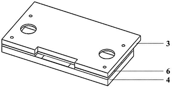
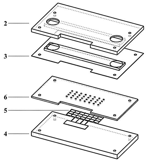
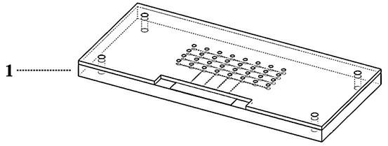
[0032] see figure 1 and figure 2 , the device is composed of a microelectrode microwell array chip 1 and a microfluidic cover sheet 2 with a top layer electrode 3 .
[0033] combine image 3 , Figure 4 , Figure 5 and Figure 6 It can be seen that the structure of the microelectrode and microhole array chip 1 is a quartz base layer 4 , a microelectrode array layer 5 and a polymer microhole array layer 6 in sequence from bottom to top.
[0034] Wherein, the microelectrode array layer 5 is obtained by processing on the quartz base layer 4 using micromachining technology (evaporation, sputtering, photolithography, etc.), and the microelectrode array layer 5 can be designed according to the flux required by the experiment. The microelectrode array of N, the diameter of microelectrode 8 is the disk of 4-6 micron, and the spacing between m...
PUM
 Abstract
Description
Claims
Application Information