A kind of solar cell structure and preparation method thereof

A solar cell and battery technology, applied in the field of solar energy, can solve the problems of poor anti-reflection effect, unfavorable cell efficiency, and improvement, and achieve the effects of increasing light intake, reducing short-wave absorption, and optimizing optical performance.

Active Publication Date: 2011-12-28
BEIJING NAURA MICROELECTRONICS EQUIP CO LTD
View PDF1 Cites 7 Cited by
  • Summary
  • Abstract
  • Description
  • Claims
  • Application Information

AI Technical Summary

Problems solved by technology

However, the optical design of this kind of double-layer film generally only considers that the wavelength band of 600-700nm has a better anti-reflection effect, and the anti-reflection effect for other wave bands is poor, and there is also a certain short-wave absorption in the passivation layer. , which is not conducive to the further improvement of battery efficiency

Method used


Image

  • A kind of solar cell structure and preparation method thereof
  • A kind of solar cell structure and preparation method thereof
  • A kind of solar cell structure and preparation method thereof

Examples


Embodiment 1

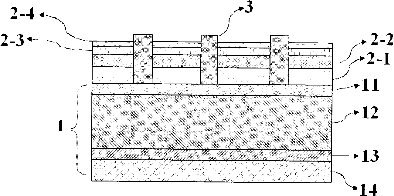
[0040] Such as figure 2 As shown, the solar cell structure of the present embodiment includes a Si battery substrate 1, and a SiNx anti-reflection passivation layer 2 is arranged on the light-facing surface of the battery substrate 1, and also includes a fired SiNx anti-reflection passivation layer 2, which is connected with the battery. Front contact electrode 3 for ohmic contact with substrate 1;

[0041] Wherein, the Si battery substrate 1 includes a P-type region 10 and an N-type region 11, and a P+ back surface field 13 and a back contact electrode 14 are formed on the back side of the Si battery substrate;

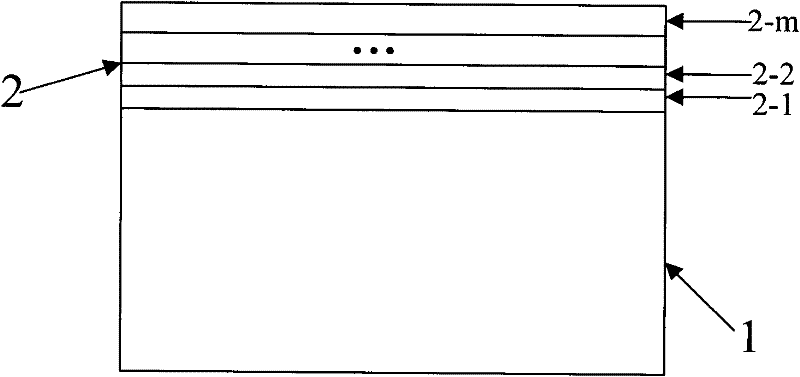
[0042] The SiNx anti-reflection passivation layer 2 includes a 4-layer film structure, along the battery substrate 1 from bottom to top are the first layer of film structure 2-1, the second layer of film structure 2-2, and the third layer of film structure 2-3 and the fourth membrane structure 2-4;

[0043] Among them, the thickness of the first film structure 2-1...

Embodiment 2

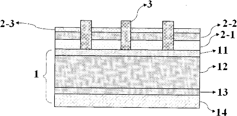
[0046] Such as image 3 As shown, the solar cell structure of the present embodiment includes a Si battery substrate 1, and a SiNx anti-reflection passivation layer 2 is arranged on the light-facing surface of the battery substrate 1, and also includes a fired SiNx anti-reflection passivation layer 2, which is connected with the battery. Front contact electrode 3 for ohmic contact with substrate 1;

[0047] Wherein, the Si battery substrate 1 includes a P-type region 10 and an N-type region 11, and a P+ back surface field 13 and a back contact electrode 14 are formed on the back side of the Si battery substrate;

[0048] The SiNx anti-reflection passivation layer 2 includes a three-layer film structure, which is the first layer film structure 2-1, the second layer film structure 2-2, and the third layer film structure 2-3 from bottom to top along the battery substrate 1. ;

[0049] Among them, the thickness of the first film structure 2-1 is about 77nm, and the refractive in...

Embodiment 3

[0072] This embodiment is a preparation method for the solar cell structure provided in Embodiment 1, as shown in Figure 5, wherein Figure 5(a) is a process flow diagram of this embodiment, and Figure 5(b) is the same as Figure 5 (a) The corresponding implementation effect diagram of the technological process, including the following steps:

[0073] S21, removing the damaged layer on the surface of the P-type silicon substrate, forming an anti-reflection surface structure and chemical cleaning.

[0074] See S21' for the implementation effect of this step.

[0075] S22, in POCl 3 The diffusion of the n-type layer is carried out in the atmosphere.

[0076] That is, an n-type layer is formed on the surface of the p-type silicon substrate, thereby producing a PN junction. The implementation effect of this step is shown in S22'.

[0077] S23, removing the peripheral PN junction.

[0078] In this step, plasma is used to etch the edge of the silicon wafer to prevent conduction on...


PUM


Abstract

The invention discloses a solar cell structure and a preparation method thereof, relating to the technical field of solar energy. The solar cell structure is invented for optimizing the optical property and the passivation property of a surface antireflection passivation layer and improving the photoelectric conversion efficiency of the cell. The solar cell structure comprises a cell substrate, wherein the sunny side of the cell substrate is provided with SiNx antireflection passivation layers of an m-layer membrane structure (m is an integer and is greater than or equal to three), wherein the first layer membrane structure is arranged on the cell substrate, the second layer membrane structure is arranged on the first layer membrane structure,..., the mth layer membrane structure is arranged on the (m-1)th layer membrane structure; the refractive index of the first layer membrane structure is greater than that of the second layer membrane structure,..., and the refractive index of the mth layer membrane structure is greater than that of the (m-1)th layer membrane structure. The solar cell structure provided by the invention can be applied to the crystal silicon cell technology.

Description

technical field [0001] The invention relates to the technical field of solar energy, in particular to a solar cell structure and a preparation method thereof. Background technique [0002] At present, solar power generation technology has received more and more attention. Among them, crystalline silicon solar cell technology occupies the leading position in solar cell technology due to its stable cell efficiency, mature process technology, simple process flow and easy mass production. The dominant position of solar cells, and will be the mainstream technology of solar cells for a long period of time in the future. [0003] In order to improve the photoelectric conversion efficiency of the crystalline silicon solar cell, a surface emission reduction passivation layer is provided on the light-facing surface of the solar cell. On the one hand, the surface emission-reducing passivation layer can reduce light reflection, increase light transmittance, and ensure that more light i...

Claims


Application Information

Patent Timeline
Patent Type & Authority Applications(China)
IPC IPC(8): H01L31/0216H01L31/042H01L31/18
CPCY02E10/52Y02E10/50Y02P70/50
Inventor 白志民
Owner BEIJING NAURA MICROELECTRONICS EQUIP CO LTD
Why Eureka
Try Eureka