
Method for preparing compound electrical contact material

A technology of electrical contact material and copper sheet, which is applied in contact materials, circuits, electrical switches, etc., can solve the problems of unclear influence of the growth of CNTs arrays on the specific action mechanism of conductive substrates and catalysts, and complicated processes, so as to improve the resistance to The effect of mechanical wear and welding resistance, improved conductivity, and overall cost-effectiveness

Inactive Publication Date: 2012-01-18
TIANJIN POLYTECHNIC UNIV
View PDF4 Cites 29 Cited by
  • Summary
  • Abstract
  • Description
  • Claims
  • Application Information

AI Technical Summary

Problems solved by technology

Recently, Nessim et al. used Fe as the catalyst, preheated the feed gas at high temperature, and placed the substrate in the low temperature area to grow CNTs directly on the Ta substrate. In this process, temperature control is the key. Keeping the substrate at a low temperature can reduce the metal matrix The reaction with the catalyst, but the specific mechanism of action between the conductive substrate and the catalyst and the influence on the growth of the CNTs array are still unclear, and the process is complicated

Method used

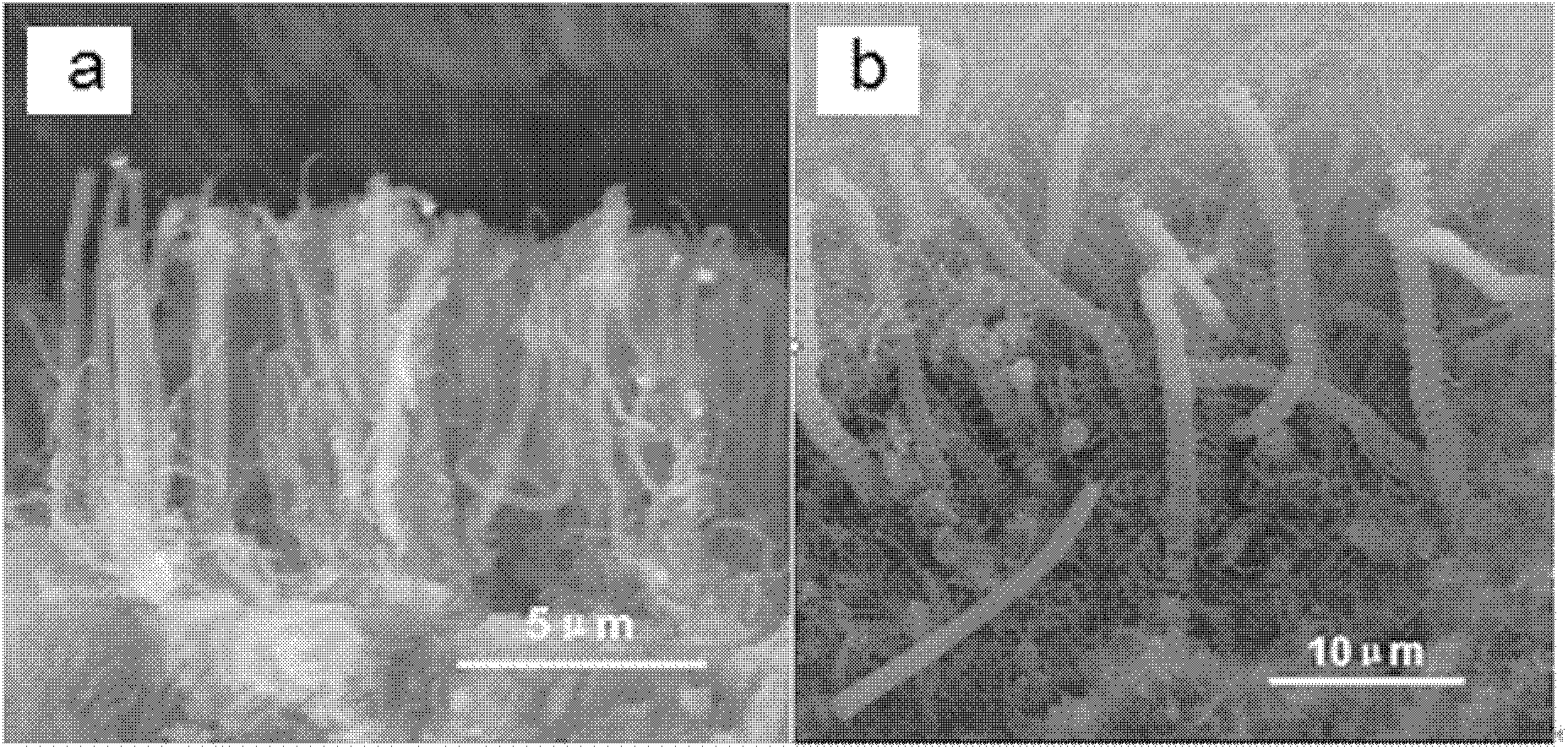
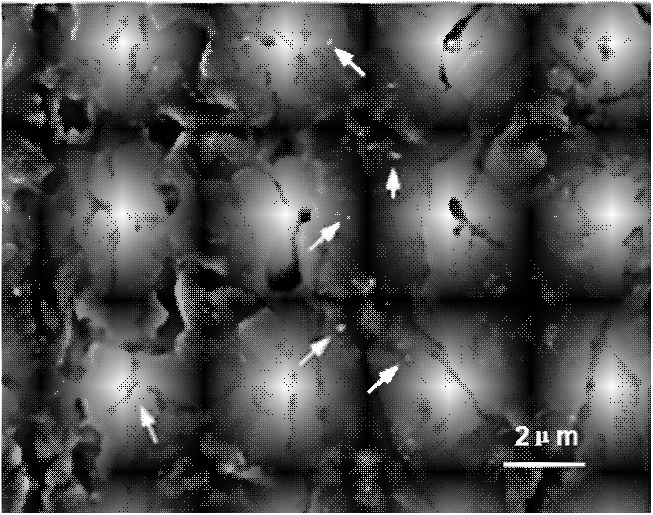

Image

  • Method for preparing compound electrical contact material
  • Method for preparing compound electrical contact material
  • Method for preparing compound electrical contact material

Examples


preparation example Construction

[0018] The preparation method (abbreviation preparation method of the composite electrical contact material of the present invention's design, see Figure 1-3 ), simply speaking, through the preparation of a new composite catalyst and precise control of the experimental process, the chemical vapor deposition technology is used to directly grow the CNTs array on the surface of the copper substrate, and then the Ag is filled into the CNTs array by impregnation, sintering and other techniques to obtain aligned CNTs. - Novel composite electrical contact material with Ag composite cladding. Its specific process is:

[0019] 1) Preparation of catalyst precursor

[0020] Embodiment Take a sample copper sheet with a diameter of 12mm and a thickness of 3mm, first use a mechanical method to polish the sample copper sheet, and then perform ultrasonic cleaning on the sample copper sheet after polishing in distilled water-acetone-alcohol, and after drying, perform plasma treatment or micr...

Embodiment 1

[0029] Mechanically polish a copper sheet with a diameter of 12mm and a thickness of 3mm. After polishing, place the copper sheet in 50ml of distilled aqueous solution for ultrasonic cleaning for 10 minutes, and then place it in 50ml of acetone solution and alcohol solution for 10 minutes. After cleaning, the copper sheet was blown dry at room temperature, and then subjected to argon plasma treatment for 0.5 min after drying. Then configure a mixed aqueous solution of nickel nitrate hexahydrate and yttrium nitrate hexahydrate as a catalyst solution, wherein the concentration of nickel nitrate is 0.0001 mol / L, and the mass ratio of nickel and yttrium Ni:Y is 1:1. Then impregnate a layer of Ni / Y catalyst solution with a concentration of 0.0001mol / L on the copper sheet treated with argon plasma, and then put the copper sheet into a vacuum drying oven and dry it under vacuum at 80°C for 1 hour to obtain Ni / Y / Cu Catalyst precursor; then the obtained Ni / Y / Cu catalyst precursor is pu...

Embodiment 2

[0031] A copper sheet with a diameter of 12 mm and a thickness of 3 mm was mechanically polished, cleaned and dried as in Example 1, and then plasma treated for 1 min. Then configure a mixed aqueous solution of nickel nitrate hexahydrate and yttrium nitrate hexahydrate as a catalyst solution, wherein the concentration of nickel nitrate is 0.02 mol / L, and the mass ratio of nickel and yttrium Ni:Y is 2:1. Then impregnate a layer of 0.02mol / L Ni / Y catalyst solution on the plasma-treated copper sheet, then put the copper sheet into a vacuum drying oven and dry it under vacuum at 100°C for 1 hour to obtain a Ni / Y / Cu catalyst precursor . Then the obtained Ni / Y / Cu catalyst precursor is put into a quartz boat, and the quartz boat is placed in the constant temperature zone in the middle of the reaction tube; Calcination for 1 hour, then the temperature was raised to 750°C, and acetylene and hydrogen (argon, hydrogen, acetylene gas flow ratio Ar:H 2 : C 2 h 2 CNTs were grown at 150s...


PUM


Abstract

The invention discloses a method for preparing a compound electrical contact material. The technical process comprises the following steps of: (1) preparing a catalyst precursor, preparing a Ni-based catalyst from a mixed aqueous solution of hexahydrated nickel nitrate and hexahydrated yttrium nitrate, and depositing on a sample copper sheet which is subjected to plasma treatment and washed to obtain a catalyst precursor, wherein the mass ratio of nickel to yttrium is 1-10; (2) preparing a CNTs (Carbon Nanotube) array, putting the catalyst precursor into a quartz boat, undergoing a decomposition reaction under the protection of argon gas, and undergoing a catalytic pyrolysis reaction to obtain a sample copper sheet on which a CNTs array grows; and (3) preparing a CNTs-Ag-Cu compound electrical contact material, adding a silver nitrate aqueous solution into the sample copper sheet on which the CNTs array grows, soaking the silver nitrate aqueous solution into the CNTs array of the sampler copper sheet under the low ultrasonic action, evaporating and decomposing repeatedly for 3-20 times for 0.2-3 hours every time till the CNTs array is fully filled.

Description

technical field [0001] The invention relates to electrical contact material technology, in particular to a method for preparing an electrical contact material in which carbon nanotubes are directly grown on a copper substrate, and the surface of the Cu substrate is covered with a CNT-Ag composite layer by dipping or other processes. Background technique [0002] The material of electrical contacts is a key factor affecting the reliability of the contact system of switching appliances. For a long time, silver-based alloys and silver metal oxides have been the main materials for the preparation of electrical contacts for low-voltage electrical appliances. Among them, AgCdO is called "universal contact", which is the first choice for electrical contacts or electrical contact materials with the best comprehensive performance, but the impact of "cadmium poisoning" on the environment has attracted people's attention. An important part of the research and development of silver-bas...

Claims


Application Information

Patent Timeline
Patent Type & Authority Applications(China)
IPC IPC(8): H01H11/04H01H1/04C01B31/02
Inventor 康建立秦凯强孙荣禄乔志军赵乃勤张虎师春生雷怡文唐英
Owner TIANJIN POLYTECHNIC UNIV
Learn More