

Method for reducing metal impurities in polysilicon
A technology of metal impurities and polysilicon, applied in the direction of non-metallic elements, chemical instruments and methods, silicon compounds, etc., can solve the problems of affecting the quality of crystals, reducing the conversion efficiency of solar cells, etc., and achieve the effect of improving the lifetime of minority carriers
- Summary
- Abstract
- Description
- Claims
- Application Information
AI Technical Summary
Problems solved by technology
Method used
Image

Examples
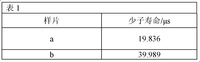
Embodiment 1
[0019] The resistivity is 0.5-3.0ohm.cm, and the P-type polysilicon wafer with a thickness of 170-200 μm is processed by the method of the present invention:
[0020] The first step, rinsing: immerse the original silicon wafer in RCAI and RCAII successively, and the ratio of RCAI solution is V NH3.H2O :V H2O2 :V DI-water =1:1:5, the ratio of RCAII solution is V HCl :V H2O2 :V DI-water =1:1:6, rinse in the solution, the temperature is 80°C, and the time is 10min;
[0021] The second step, drying: place the rinsed silicon wafer in deionized water and dry it with nitrogen;
[0022] The third step, rapid heat treatment: place the dried silicon wafer in a rapid heat treatment furnace for rapid heat treatment under nitrogen atmosphere, heating rate: 70°C / s, holding time: 3min, cooling rate: 200°C / s;
[0023] The fourth step, gettering: put the above-mentioned silicon wafer in a diffusion furnace for single-sided phosphorus expansion. The temperature of phosphorus expansion is ...
PUM
| Property | Measurement | Unit |
|---|---|---|
| thickness | aaaaa | aaaaa |
| thickness | aaaaa | aaaaa |
Abstract
Description
Claims
Application Information