Method for manufacturing laser chip for water vapor detection

A manufacturing method and laser technology, applied in lasers, laser parts, semiconductor lasers, etc., can solve the problems of increased optical loss and decreased laser performance.

Inactive Publication Date: 2012-02-29
INST OF SEMICONDUCTORS - CHINESE ACAD OF SCI
View PDF1 Cites 3 Cited by
  • Summary
  • Abstract
  • Description
  • Claims
  • Application Information

AI Technical Summary

Problems solved by technology

As the wavelength of DFB laser increases, the optical loss caused by Auger recombination, interband absorption, etc. also increases, which leads to the degradation of laser performance

Method used


Image

  • Method for manufacturing laser chip for water vapor detection
  • Method for manufacturing laser chip for water vapor detection
  • Method for manufacturing laser chip for water vapor detection

Examples


Embodiment Construction

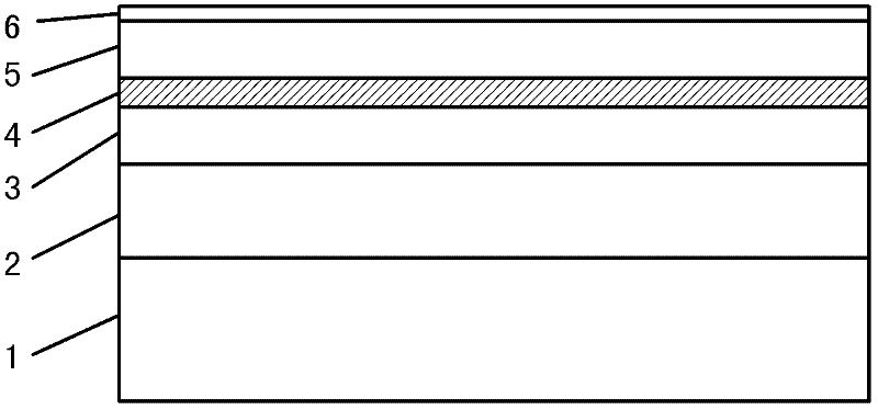
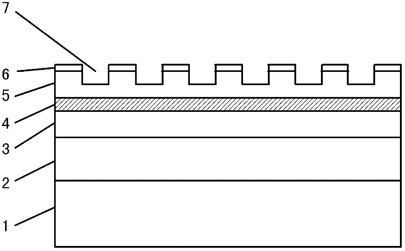
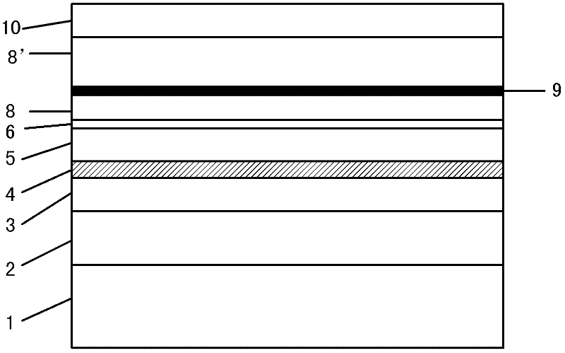
[0023] See Figure 1 to Figure 6 , The manufacturing method of the laser chip for water vapor detection of the present invention, the specific implementation steps are as follows:

[0024] Step 1: Using low pressure metal organic chemical vapor deposition (LP-MOCVD), the InP buffer layer 2, the lower waveguide layer 3, and the multiple quantum well structure are sequentially grown on the (001) surface of the n-InP substrate 1 in the same epitaxy 4. The upper waveguide layer 5 and the pn inversion layer 6;

[0025] Among them, the growth temperature used in the low-pressure metal organic metal organic chemical vapor epitaxy growth is 655° C., and the growth pressure is 22 mbar. This method has low cost and is suitable for large-scale production;

[0026] Wherein, the thickness of the InP buffer layer 2 is 1 μm, and the doping concentration is 1×10 18 / cm 3 ;

[0027] Wherein, the compressively strained quantum well material in the multiple quantum well structure 4 is InGaAs, the strai...


PUM

PropertyMeasurementUnit
Bandgap wavelengthaaaaaaaaaa

Abstract

The invention discloses a method for manufacturing a laser chip for water vapor detection. The method comprises the following steps of: 1, epitaxially growing an InP buffer layer, a lower waveguide layer, a multi-quantum well structure, an upper waveguide layer and a p-n inversion layer on an n-type InP substrate sequentially; 2, making a recoupling grating on the p-n inversion layer and the upper waveguide layer by using a holographic exposure method; 3, secondarily epitaxially growing a first p-InP cover layer, an etching stop layer, a second p-InP cover layer and a p-InGaAs contact layer on the recoupling grating; 4, corroding to form a ridge-type waveguide structure on the second p-InP cover layer and the p-InGaAs contact layer, and depositing a silicon dioxide layer in a large area; 5, etching the silicon dioxide layer in the middle of the ridge-type waveguide structure so as to form a window; and 6, sputtering to form a P-surface electrode and evaporating to form an N-surface electrode on the surfaces of the ridge-type waveguide structure and the window.

Description

Technical field [0001] The invention relates to the technical field of semiconductor laser detectors, in particular to a method for manufacturing a laser chip for water vapor detection that uses InGaAlAs material with a large conduction band energy difference as a barrier in a quantum well structure and combines conventional wet etching and photolithography processes . Background technique [0002] Our country has a vast territory and relatively complicated meteorological phenomena. Natural disasters (such as freezing rain and snow, heavy rains in summer) occur from time to time. Once they occur, the country will suffer heavy losses. The importance of weather forecasting is self-evident. Water vapor is one of the four major elements of atmospheric detection. If it can be accurately detected in real time, it is of great significance to the accuracy of weather forecasts. At present, electric hygrometers are mainly used at home and abroad to measure atmospheric humidity, such as th...

Claims


Application Information

Patent Timeline
IPC IPC(8): H01S5/343H01S5/22
Inventor 于红艳周旭亮邵永波王宝军潘教青王圩
Owner INST OF SEMICONDUCTORS - CHINESE ACAD OF SCI
Why Eureka
Try Eureka