Strained multiple quantum well laser based on gesn/sigesn material and its fabrication method

A strained multi-quantum well and laser technology, applied in the field of optoelectronics, can solve the problems of increasing the carrier concentration, weakening the optical gain of the laser, increasing the threshold of the laser, etc. Effect

Active Publication Date: 2019-05-31
XIDIAN UNIV
View PDF2 Cites 0 Cited by
  • Summary
  • Abstract
  • Description
  • Claims
  • Application Information

AI Technical Summary

Problems solved by technology

However, as the thickness of the active region decreases, its optical confinement factor will drop sharply, which will weaken the optical gain of the laser. In addition, the threshold energy of the laser in the potential well will increase, which will increase the carrier concentration to a certain extent. demand and blue shift the laser

Method used


Image

  • Strained multiple quantum well laser based on gesn/sigesn material and its fabrication method
  • Strained multiple quantum well laser based on gesn/sigesn material and its fabrication method

Examples


Embodiment

[0043] Example: Ge 0.9 sn 0.1 / Ge 0.695 Si 0.161 sn 0.144 Fabrication method of strained multiple quantum well laser.

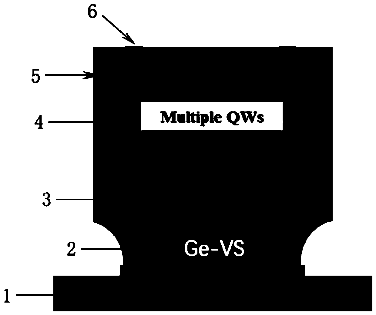
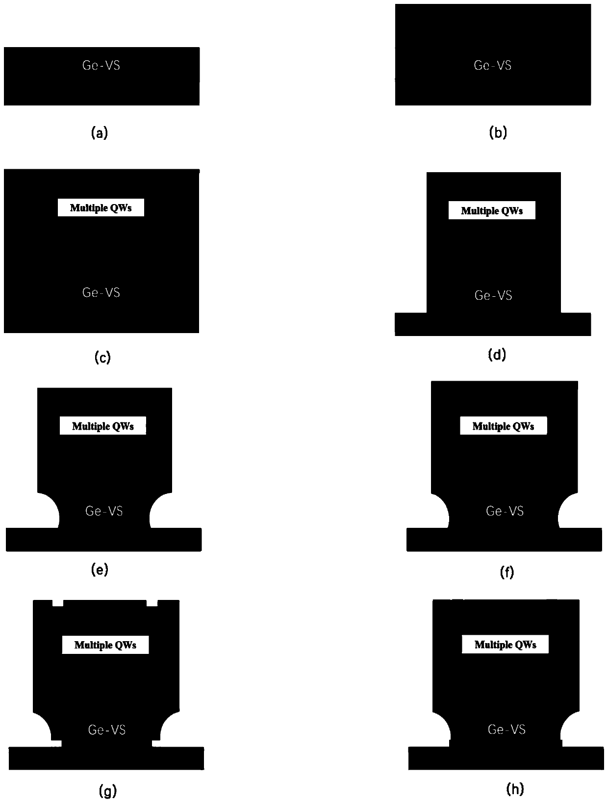
[0044] Step 1: Prepare a Ge pseudosubstrate.

[0045] Using the solid-source molecular beam epitaxy process, on the undoped (100) Si substrate (1), the GeH 4 As a Ge source, after growing a 30nm thick Ge buffer layer in an environment of 350°C, the temperature was quickly raised to 600°C and epitaxially grown several hundred nanometers of Ge film as a pseudo-substrate such as figure 2 (a);

[0046] Step 2: Phosphorus ion implantation.

[0047] At an energy of 50KeV and an implant dose of 10 15 cm -2 , The implanted ions are P(31) under the condition that the substrate is tilted at an angle of 7° + Phosphorus ion implantation process to form Ge N + Type pseudosubstrate (2);

[0048] Step 3: Prepare a GeSn buffer layer.

[0049] Using low-temperature solid-source molecular beam epitaxy, the Ge N + Intrinsic Ge with a thickness of 100nm was epitax...


PUM


Abstract

The invention discloses a strain multiple quantum well laser device based on GeSn / SiGeSn material and a manufacturing method thereof. A barrier layer adopts a GeSiSn material; and the barrier layer adopts a GeSn material. A pseudo substrate (Ge), a buffer layer (GeSn) and an active area (GeSn / GeSiSn) are vertically distributed on a substrate (Si) from bottom to top in sequence, and an Si3N4 tensile stress film is wrapped around the pseudo substrate, the buffer layer and the active area. The manufacturing method of the laser device disclosed by the invention comprises the following steps: (1) adopting a low-temperature solid-source molecular beam epitaxy growth technology to grow the GeSn and GeSiSn materials; and (2) adopting a standard laser device manufacturing technology to process the device. Through a multiple quantum well structure and the tensile strain introduced by the additionally added Si3N4 stress film, red shift occurs for the laser wavelength of the laser device, the optical gain of the laser device is obviously improved, and the threshold value is greatly reduced.

Description

technical field [0001] The invention belongs to the field of optoelectronic technology, and further relates to a GeSn / SiGeSn material-based strained multi-quantum well laser and a manufacturing method thereof in the field of semiconductor infrared light sources. The invention can be used as a novel mid-infrared light source in a mid-infrared optoelectronic integrated system. Background technique [0002] With the continuous development of microelectronics and optoelectronics technology, the problem of mid-infrared light source has become one of the challenges it faces in silicon-based mid-infrared optoelectronic integrated systems. [0003] Traditional group IV materials and alloys compatible with Si are indirect bandgap semiconductors, and the lowest point of the conduction band deviates from the highest point of the valence band in the reciprocal space. The recombination in indirect bandgap materials is mainly indirect recombination, and the assistance of phonons is neede...

Claims


Application Information

Patent Timeline
Patent Type & Authority Patents(China)
IPC IPC(8): H01S5/34
CPCH01S5/3426
Inventor 刘艳高曦韩根全郝跃张庆芳
Owner XIDIAN UNIV
Why Eureka
Try Eureka