Manufacturing method for back contact type silicon solar cell

A silicon solar cell and back contact technology, which is applied in the manufacture of circuits, electrical components, and final products, can solve problems affecting the mechanical strength of devices, complex manufacturing processes, and broken silicon wafers, so as to improve photoelectric conversion efficiency and simplify the manufacturing process. , the effect of reducing the fragmentation rate

Active Publication Date: 2014-05-14
CSI CELLS CO LTD +1
View PDF25 Cites 0 Cited by
  • Summary
  • Abstract
  • Description
  • Claims
  • Application Information

AI Technical Summary

Problems solved by technology

Although this technology avoids the shading loss caused by the front electrode, in order to ensure that the current on the light-receiving surface is transmitted to the back without loss, tens of thousands of holes need to be set, and high-concentration doping needs to be formed in the holes. These conditions have led to its preparation. The process is very complicated and the cost is high; at the same time, too many holes also affect the mechanical strength of the device, and a large number of silicon wafers will be broken during production

Method used


Image

  • Manufacturing method for back contact type silicon solar cell
  • Manufacturing method for back contact type silicon solar cell
  • Manufacturing method for back contact type silicon solar cell

Examples


Embodiment 1

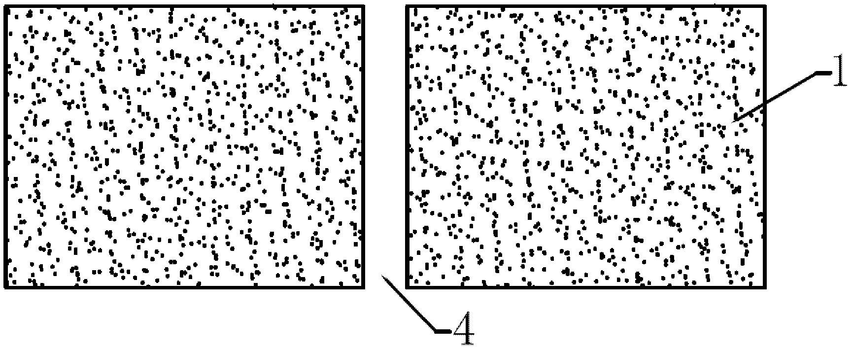
[0039] see figure 1 Shown in ~9, a kind of preparation method of back contact silicon solar cell, silicon chip is n-type, comprises the following steps:

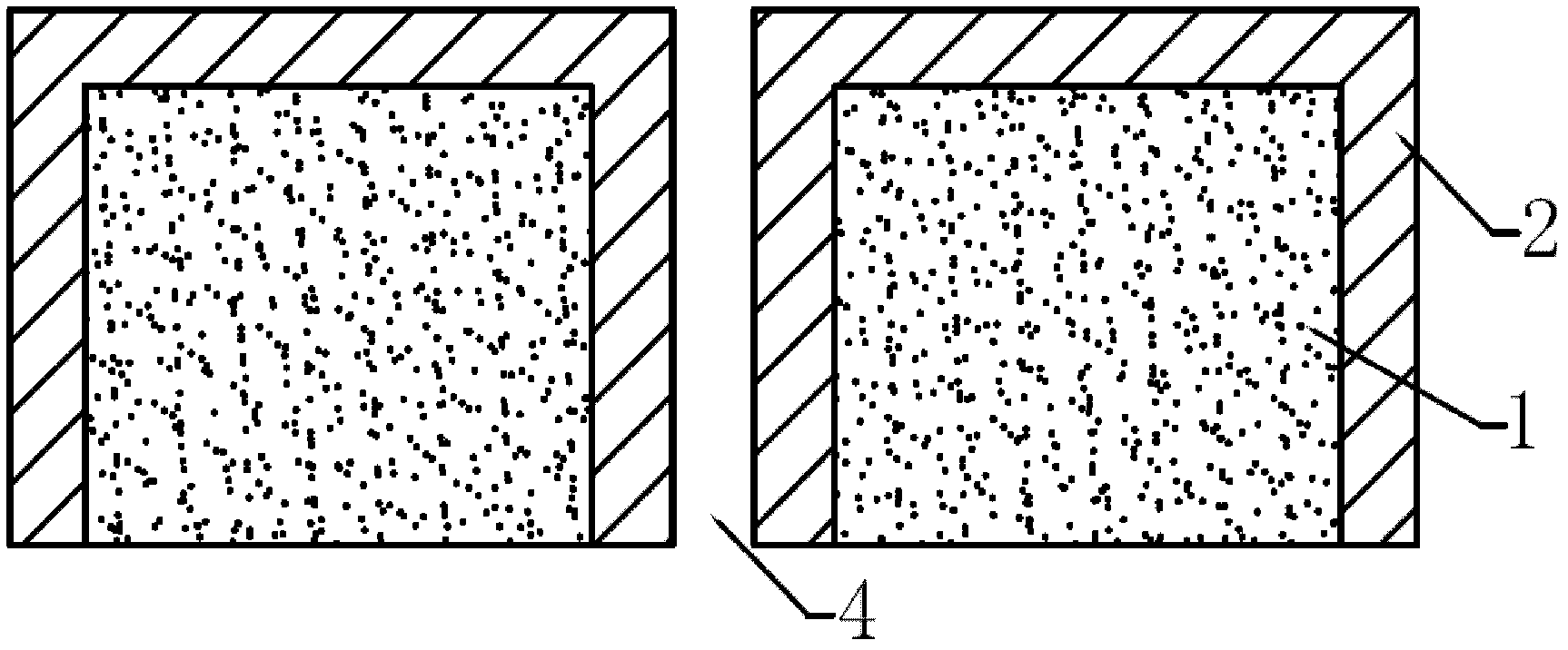
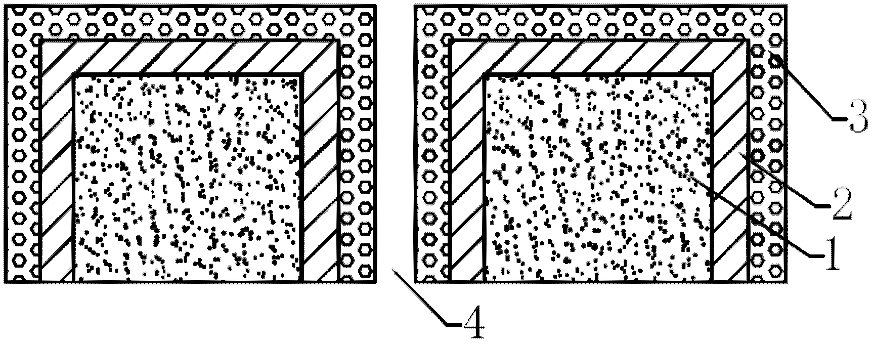
[0040](1) Holes 4 are opened on the surface of the silicon wafer, the number of which is 60. Its function is to set electrodes in the holes to lead the current from the light-receiving surface of the battery to the backlight surface of the battery, so that the positive and negative electrodes of the battery can be They are all located on the back of the battery sheet; in this embodiment, laser, mechanical drilling or chemical etching can be used to open holes; The uneven structure is formed on the surface to extend the propagation path of light on the surface, thereby improving the absorption of light by the silicon wafer; the schematic diagram of the silicon wafer structure after opening is as follows figure 1 shown;

[0041] (2) Boron diffusion is carried out on the surface of the silicon wafer, and the PN junction 2 i...

Embodiment 2

[0051] A method for preparing a back-contact silicon solar cell, the silicon wafer is p-type, comprising the steps of:

[0052] The first step is to open holes on the silicon wafer, the number of which is 100. Its function is to set electrodes in the through holes to lead the current from the light-receiving side of the battery to the backlight of the battery, so that the positive electrode and the backlight of the battery can be connected to each other. The negative electrodes are all located on the back of the battery sheet; in this embodiment, laser, mechanical drilling or chemical etching can be used to open holes;

[0053] The second step is texturing; its purpose is to form a rough structure on the surface of the original bright silicon wafer through chemical reaction to prolong the propagation path of light on its surface, thereby improving the absorption of light by the silicon wafer;

[0054] The third step is to diffuse phosphorus on the surface of the silicon wafer ...


PUM


Abstract

The invention relates to a manufacturing method for a back contact silicon solar cell, which comprises the following steps of: (1) setting holes on the surface of silicon wafers, and etching textures on the light receiving surfaces of the silicon wafers; (2) diffusing on the light receiving surfaces of the silicon wafers to make junctions, and forming PN junctions in the light receiving surfaces, the peripheries and holes of the silicon wafers; (3) setting transparent conductive films on the PN junctions in the light receiving surfaces, the peripheries and holes of the silicon wafers; (4) etching the peripheries of the silicon wafers to remove the transparent conductive films and the PN junctions on the peripheries of the silicon wafers, and coating antireflection films on the transparent conductive films in the light receiving surfaces of the silicon wafers; and (5) preparing through hole electrodes, back metal electrodes and back passivation fields on the non film coated surfaces of the silicon wafers to obtain the back contact silicon solar cells. The light receiving surfaces of the back contact silicon solar cells are not covered with electrodes, so that the shading loss is avoided, and the photoelectric conversion efficiency is remarkably improved; holes to be arranged are also greatly reduced, so that the fragmentation rate is greatly reduced; and the manufacturing process is simplified.

Description

technical field [0001] The invention relates to a method for preparing a back-contact silicon solar cell, belonging to the field of crystalline silicon solar cell manufacturing. Background technique [0002] Conventional fossil fuels are being exhausted day by day. Among the existing sustainable energy sources, solar energy is undoubtedly the cleanest, most common and most potential alternative energy source. At present, among all solar cells, silicon solar cells are one of the solar cells that have been widely commercialized. This is due to the extremely abundant reserves of silicon materials in the earth's crust. With excellent electrical and mechanical properties, silicon solar cells occupy an important position in the field of photovoltaics. Therefore, developing cost-effective silicon solar cells has become one of the main research directions of photovoltaic companies in various countries. [0003] The power generation principle of silicon solar cells is based on the ...

Claims


Application Information

Patent Timeline
Patent Type & Authority Patents(China)
IPC IPC(8): H01L31/18
CPCY02P70/50
Inventor 吴坚王栩生章灵军
Owner CSI CELLS CO LTD
Why Eureka
Try Eureka