Preparation method for graphical sapphire substrate
A patterned sapphire and patterned technology, which is applied in semiconductor devices, electrical components, circuits, etc., can solve the problems of unfavorable epitaxial layer crystal quality, pollution, and improvement, and achieve the reduction of linear dislocation density, good light transmittance, chemical and the effect of stabilizing physical properties
- Summary
- Abstract
- Description
- Claims
- Application Information
AI Technical Summary
Problems solved by technology
Method used
Image
Examples
Embodiment 1
[0043] Prepare a patterned sapphire substrate for nitride epitaxial growth in the following order:
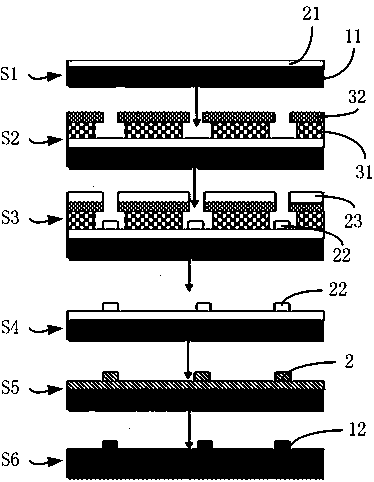
[0044] (1) Sputtering metal aluminum film: use DC magnetron sputtering technology to magnetron sputter about 10nm metal aluminum film on one surface of the sapphire substrate.
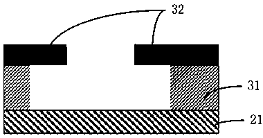
[0045] (2) Electron beam lithography: spin-coat the first layer of P (MMA-MAA) photoresist on the aluminum film of the sapphire substrate sputtered with the metal aluminum film in step (1), the thickness is about 250nm, and the spinning speed is 2000 r / min , and dry at 150°C for 15 minutes; then spin-coat the second layer of PMMA photoresist on the dried first layer of P(MMA-MAA) photoresist, with a thickness of about 150nm, and spin the glue at a speed of 2000 r / min. Dry at 180°C for 10 minutes; then use a 150-Turnkey direct-writing electron beam exposure machine from Raith, Germany for electron beam exposure. The exposure pattern is designed as a periodic circle, the radius of the exposure area is 300...
Embodiment 2
[0051] Prepare a patterned sapphire substrate for nitride epitaxial growth in the following order:
[0052] (1) Sputtering metal aluminum film: use DC magnetron sputtering technology to magnetron sputter about 10nm metal aluminum film on one surface of the sapphire substrate.
[0053] (2) Electron beam lithography: spin-coat the first layer of P (MMA-MAA) photoresist on the aluminum film of the sapphire substrate sputtered with the metal aluminum film in step (1), the thickness is about 250nm, and the spinning speed is 2000 r / min , and dry at 150°C for 15 minutes; then spin-coat the second layer of PMMA photoresist on the dried first layer of P(MMA-MAA) photoresist, with a thickness of about 150nm, and spin the glue at a speed of 2000 r / min. Dry at 180°C for 10 minutes; then use the 150-Turnkey direct-writing electron beam exposure machine of Raith Company in Germany for electron beam exposure. , MIBK: IPA=1:3 developing 60s, IPA fixing 20s, N 2 Blow dry to obtain electron b...
Embodiment 3
[0059] Prepare a patterned sapphire substrate for nitride epitaxial growth in the following order:
[0060] (1) Sputtering metal aluminum film: use DC magnetron sputtering technology to magnetron sputter about 10nm metal aluminum film on one surface of the sapphire substrate.
[0061] (2) Electron beam lithography: spin-coat the first layer of P (MMA-MAA) photoresist on the aluminum film of the sapphire substrate sputtered with the metal aluminum film in step (1), the thickness is about 250nm, and the spinning speed is 2000 r / min , and dry at 150°C for 15 minutes; then spin-coat the second layer of PMMA photoresist on the dried first layer of P(MMA-MAA) photoresist, with a thickness of about 150nm, and spin the glue at a speed of 2000 r / min. Dry at 180°C for 10 minutes; then use a 150-Turnkey direct-writing electron beam exposure machine from Raith, Germany for electron beam exposure. The exposure pattern is designed as a periodic circle, the radius of the exposure area is 300...
PUM
| Property | Measurement | Unit |
|---|---|---|
| thickness | aaaaa | aaaaa |
| thickness | aaaaa | aaaaa |
| thickness | aaaaa | aaaaa |
Abstract
Description
Claims
Application Information


