Preparation method for graphical sapphire substrate

A patterned sapphire and patterned technology, applied in semiconductor devices, electrical components, circuits, etc., can solve problems such as pollution, unfavorable epitaxial layer crystal quality, damage, etc., achieve the effect of simple and easy process, and overcome pattern distortion

Active Publication Date: 2012-04-04
HARBIN INST OF TECH SHENZHEN GRADUATE SCHOOL
View PDF2 Cites 19 Cited by
  • Summary
  • Abstract
  • Description
  • Claims
  • Application Information

AI Technical Summary

Problems solved by technology

However, dry etching is easy to cause certain pollution and damage to the surface of the sapphire substrate, especially the edge of the mesa, which is not conducive to the further improvement of the crystal quality of the epitaxial layer

Method used


Image

  • Preparation method for graphical sapphire substrate
  • Preparation method for graphical sapphire substrate
  • Preparation method for graphical sapphire substrate

Examples


Embodiment 1

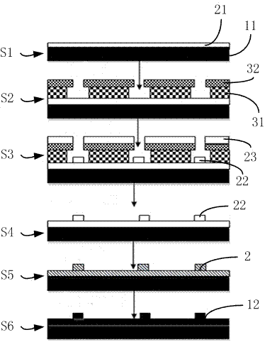
[0043] Prepare a patterned sapphire substrate for nitride epitaxial growth in the following order:

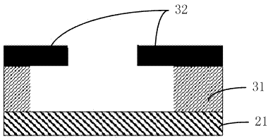
[0044] (1) Sputtering metal aluminum film: use DC magnetron sputtering technology to magnetron sputter about 10nm metal aluminum film on one surface of the sapphire substrate.

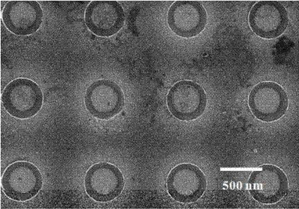
[0045] (2) Electron beam lithography: spin-coat the first layer of P (MMA-MAA) photoresist on the aluminum film of the sapphire substrate sputtered with the metal aluminum film in step (1), the thickness is about 250nm, and the spinning speed is 2000 r / min , and dry at 150°C for 15 minutes; then spin-coat the second layer of PMMA photoresist on the dried first layer of P(MMA-MAA) photoresist, with a thickness of about 150nm, and spin the glue at a speed of 2000 r / min. Dry at 180°C for 10 minutes; then use a 150-Turnkey direct-writing electron beam exposure machine from Raith, Germany for electron beam exposure. The exposure pattern is designed as a periodic circle, the radius of the exposure area is 300...

Embodiment 2

[0051] Prepare a patterned sapphire substrate for nitride epitaxial growth in the following order:

[0052] (1) Sputtering metal aluminum film: use DC magnetron sputtering technology to magnetron sputter about 10nm metal aluminum film on one surface of the sapphire substrate.

[0053] (2) Electron beam lithography: spin-coat the first layer of P (MMA-MAA) photoresist on the aluminum film of the sapphire substrate sputtered with the metal aluminum film in step (1), the thickness is about 250nm, and the spinning speed is 2000 r / min , and dry at 150°C for 15 minutes; then spin-coat the second layer of PMMA photoresist on the dried first layer of P(MMA-MAA) photoresist, with a thickness of about 150nm, and spin the glue at a speed of 2000 r / min. Dry at 180°C for 10 minutes; then use the 150-Turnkey direct-writing electron beam exposure machine of Raith Company in Germany for electron beam exposure. , MIBK: IPA=1:3 developing 60s, IPA fixing 20s, N 2 Blow dry to obtain electron b...

Embodiment 3

[0059] Prepare a patterned sapphire substrate for nitride epitaxial growth in the following order:

[0060] (1) Sputtering metal aluminum film: use DC magnetron sputtering technology to magnetron sputter about 10nm metal aluminum film on one surface of the sapphire substrate.

[0061] (2) Electron beam lithography: spin-coat the first layer of P (MMA-MAA) photoresist on the aluminum film of the sapphire substrate sputtered with the metal aluminum film in step (1), the thickness is about 250nm, and the spinning speed is 2000 r / min , and dry at 150°C for 15 minutes; then spin-coat the second layer of PMMA photoresist on the dried first layer of P(MMA-MAA) photoresist, with a thickness of about 150nm, and spin the glue at a speed of 2000 r / min. Dry at 180°C for 10 minutes; then use a 150-Turnkey direct-writing electron beam exposure machine from Raith, Germany for electron beam exposure. The exposure pattern is designed as a periodic circle, the radius of the exposure area is 300...


PUM

PropertyMeasurementUnit
thicknessaaaaaaaaaa
thicknessaaaaaaaaaa
thicknessaaaaaaaaaa

Abstract

The invention relates to a preparation method for graphical sapphire substrate for epitaxial growth of nitride, which comprises the following steps of: firstly, magnetron sputtering a layer of aluminous film on the sapphire substrate; next, coating two layers of photoresist films and the lower layer of photoresist film has better photosensitivity; next, exposing and developing the substrate to form a photoresist film graph; then carrying out magnetron sputtering to a second layer of aluminous film, and dipping the aluminous film in solvent to remove the outer layer aluminous film; finally processing the substrate at lower temperature and then high temperature to form the graphical sapphire substrate with single crystal alumina film. The preparation method is simple and easy to implement, which overcomes the problems that the dry etching method will pollute and damage substrate as well as overcomes the problems that the wet etching method will cause graphic distortion.

Description

technical field [0001] The invention relates to a preparation process of an epitaxial wafer, in particular to a preparation method of a patterned sapphire substrate used for epitaxial growth at nitride. Background technique [0002] In recent years, high-brightness and high-power nitride light-emitting diodes (LEDs) have attracted much attention, and they are widely used in traffic lights, LCD backlights, solid-state lighting, and full-color display screens. These commercial products require LEDs to have excellent performance in terms of luminance and luminous efficiency. Sapphire has the advantages of stable chemical and physical properties, good light transmission, and reasonable cost, so it is widely used in nitride epitaxial substrates. However, due to the huge difference in lattice constant mismatch and thermal expansion coefficient mismatch between the nitride epitaxial film and the sapphire substrate at the bottom, the use of hydride vapor phase epitaxy (HVPE), metal...

Claims


Application Information

Patent Timeline
Patent Type & Authority Applications(China)
IPC IPC(8): H01L33/00
Inventor 张化宇汪桂根崔林韩杰才
Owner HARBIN INST OF TECH SHENZHEN GRADUATE SCHOOL
Why Eureka
Try Eureka