

Device and method for etching copper conducting film on glass substrate ink by using pulse laser
A glass substrate, pulsed laser technology, used in laser welding equipment, welding equipment, metal processing equipment, etc., can solve the problems of low processing efficiency, poor selectivity, and large footprint
- Summary
- Abstract
- Description
- Claims
- Application Information
AI Technical Summary
Problems solved by technology
Method used
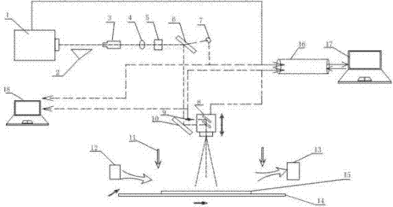
Image


Examples
Embodiment Construction
[0014] The invention uses laser etching copper conductive film and ITO thin film material of electronic products, adopts high-frequency pulse laser, the processed material is copper film and ITO material with high conductivity, and the laser is focused on the copper film and ITO thin film material, so as to achieve etching Effect.
[0015] The processing material film layers are glass substrate, black ink, total reflection dielectric film, ITO and copper conductive film from bottom to top. When the high-frequency pulsed laser is focused on the upper surface of the copper film and the device is etching, after reaching the removal energy threshold of the material, the copper film and ITO thin film materials are vaporized under the action of the high-frequency pulsed laser to achieve the etching process. Purpose, when the copper film and ITO are etched completely, when the high-frequency pulsed laser acts on the total reflection dielectric film of the laser wavelength, according ...
PUM
| Property | Measurement | Unit |
|---|---|---|
| Wavelength | aaaaa | aaaaa |
| Pulse width | aaaaa | aaaaa |
Abstract
Description
Claims
Application Information