One-time programmable read-only memory for CMOS (Complementary Metal Oxide Semiconductor) and manufacturing method thereof

A technology of read-only memory and manufacturing method, applied in semiconductor/solid-state device manufacturing, electric solid-state device, semiconductor device and other directions, can solve the problems of good floating gate wrapping, loss, exposed edge of OTPROM floating gate, etc., to achieve stable and reliable process , the effect of good performance

Inactive Publication Date: 2012-04-25
ADVANCED SEMICON MFG CO LTD
View PDF4 Cites 19 Cited by
  • Summary
  • Abstract
  • Description
  • Claims
  • Application Information

AI Technical Summary

Problems solved by technology

[0004] The sidewall in the current 0.35μm CMOS process is silicon dioxide (LPTEOS) forming a shoulder type (shoulder type), and the top of the shoulder type silicon dioxide (LPTEOS) sidewall is silicon dioxide (silicon dioxide) at the contact with the OTP ROM floating gate LPTEOS) is very thin, especially the cleaning-related steps in the subsequent process will lose the silicon dioxide (LPTEOS) of the sidewall of the OTP ROM floating gate, resulting in the exposed edge of the OTP ROM floating gate
The formation of metal silicide is a self-alignment process. Metal silicide is not formed on the surface of the floating gate of CMOS OTP ROM. In the process, the silicon dioxide

Method used


Image

  • One-time programmable read-only memory for CMOS (Complementary Metal Oxide Semiconductor) and manufacturing method thereof
  • One-time programmable read-only memory for CMOS (Complementary Metal Oxide Semiconductor) and manufacturing method thereof
  • One-time programmable read-only memory for CMOS (Complementary Metal Oxide Semiconductor) and manufacturing method thereof

Examples


Embodiment Construction

[0050]The present invention will be further described below in conjunction with specific embodiment and accompanying drawing, set forth more details in the following description so as to fully understand the present invention, but the present invention can obviously be implemented in a variety of other ways different from this description, Those skilled in the art can make similar promotions and deductions based on actual application situations without violating the connotation of the present invention, so the content of this specific embodiment should not limit the protection scope of the present invention.

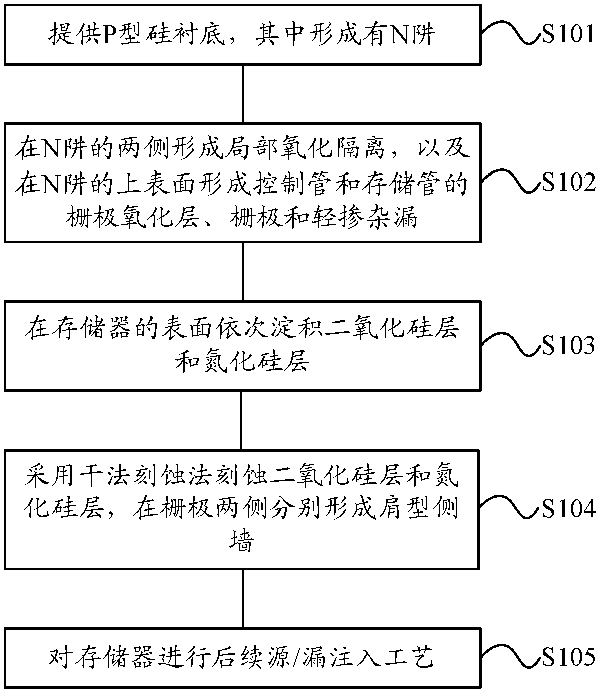
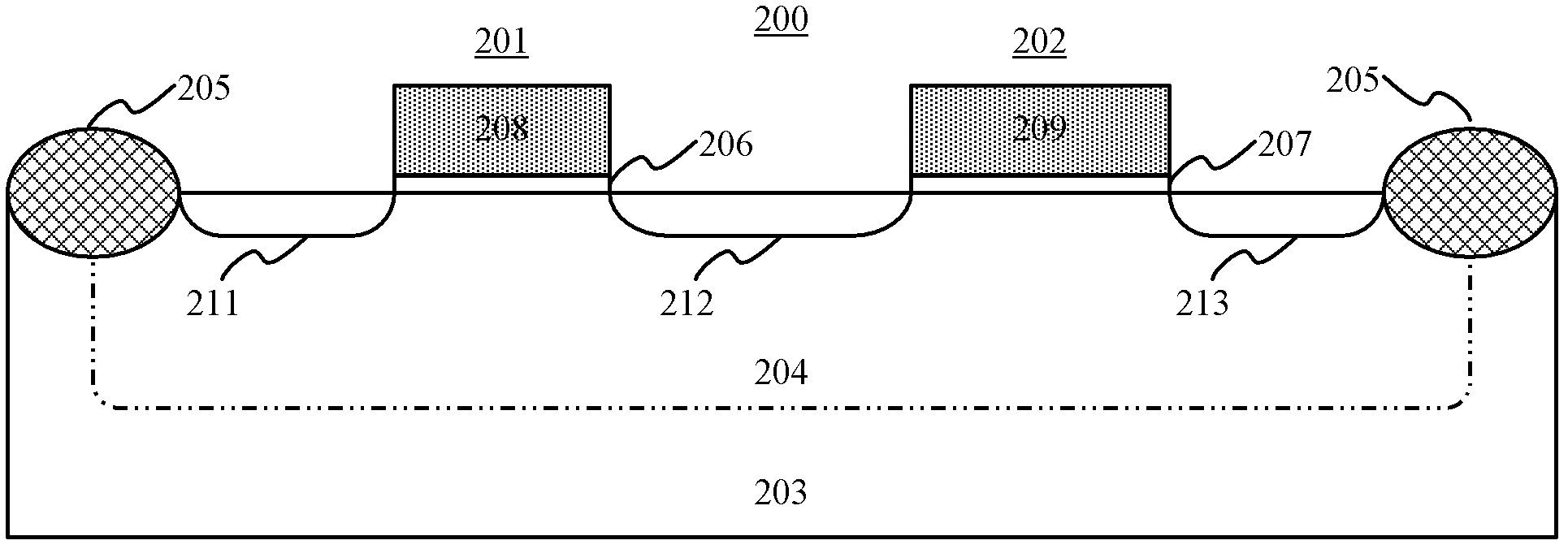
[0051] figure 1 It is a flowchart of a manufacturing method of a CMOS one-time programmable read-only memory according to an embodiment of the present invention. Such as figure 1 As shown, the manufacturing method may include:

[0052] Executing step S101, providing a P-type silicon substrate in which an N well is formed;

[0053] Execute step S102, forming local oxid...


PUM


Abstract

The invention provides a one-time programmable read-only memory for a CMOS (Complementary Metal Oxide Semiconductor) and a manufacturing method of the one-time programmable read-only memory. The memory comprises a control tube and a memory tube; the manufacturing method comprises the following steps of: providing a P-type silicon substrate, and forming a N-well in the P-type silicon substrate; forming local oxide isolation at two sides of the N-well, forming grid electrode oxidation layers, grid electrodes and lightly-doped drains of the control tube and the memory tube on the P-type silicon substrate and the upper surface of the N-well; sequentially depositing a silicon dioxide layer and a silicon nitride layer on the surface of the memory; etching the silicon dioxide layer and the silicon nitride layer by adopting a dry etching method, and respectively forming shoulder-type spacers at two sides of the grid electrode; and carrying out a follow-up source/drain injection technology on the memory. According to the manufacturing method, the OTP ROM (one-time programmable read-only memory) which is optimized through a sidewall and silicide barrier layer (SBK) technology has good performance and is greatly improved in terms of reliability, particularly the data retention performance of electric charges; and the technology is stale and reliable.

Description

technical field [0001] The invention relates to the technical field of semiconductor device manufacturing, in particular, the invention relates to a CMOS one-time programmable read-only memory (OTP ROM) and a manufacturing method thereof. Background technique [0002] One-time programmable read-only memory (OTP ROM) is a type of memory in microcontrollers (MCUs). The MCU with mask read-only memory (Mask ROM) is cheap, but the program has been solidified when it leaves the factory, which is suitable for applications where the program is fixed. The MCU program of flash memory (Flash) and electrically erasable programmable read-only memory (EEPROM) can be repeatedly erased and written, which is very flexible, but the structure and process are complex, the development cycle is long, and the price is high. It is suitable for those who are not sensitive to price or require Very high application occasions or for development purposes. The MCU price of OTPROM is between the two, an...

Claims


Application Information

Patent Timeline
IPC IPC(8): H01L21/8246H01L27/112
Inventor 刘建华
Owner ADVANCED SEMICON MFG CO LTD
Why Eureka
Try Eureka