Machining method of blind hole PCB (Printed Circuit Board)
A technology of a PCB board and a processing method, which is applied to the processing field of blind-hole PCB boards, can solve the problems of uneven copper layer, uneven thickness of copper layer, uneven thickness of copper reduction, etc., and achieve uniform thickness distribution and thinning of conductive layer. The effect of thickness
- Summary
- Abstract
- Description
- Claims
- Application Information
AI Technical Summary
Problems solved by technology
Method used
Image
Examples
Embodiment Construction
[0025] The following will clearly and completely describe the technical solutions in the embodiments of the present invention with reference to the accompanying drawings in the embodiments of the present invention. Obviously, the described embodiments are only some, not all, embodiments of the present invention. Based on the embodiments of the present invention, all other embodiments obtained by persons of ordinary skill in the art without creative efforts fall within the protection scope of the present invention.
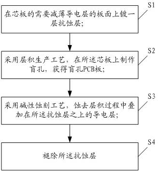
[0026] see figure 1 , is the schematic flow chart of an embodiment of the processing method of blind hole PCB board provided by the present invention, and this method comprises the following steps:
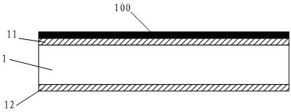
[0027] S1. Coating a resist layer on the surface of the core board where the conductive layer needs to be thinned;
[0028] S2. Using a layered production process, making blind holes on the core board to obtain a blind hole PCB board;
[0029] S3, using an alkaline e...
PUM
 Abstract
Description
Claims
Application Information


