Method for preparing nano structure on surface of (111) silicon wafer

A nanostructure, silicon wafer surface technology, applied in nanotechnology, chemical instruments and methods, semiconductor/solid-state device manufacturing, etc., can solve the problems of high preparation cost, expensive SOI silicon wafer material, and single nanowire structure of the preparation object. Achieve the effect of good crystal alignment, complete lattice structure and good scale uniformity

Inactive Publication Date: 2012-05-02
SHANGHAI INST OF MICROSYSTEM & INFORMATION TECH CHINESE ACAD OF SCI
View PDF5 Cites 13 Cited by
  • Summary
  • Abstract
  • Description
  • Claims
  • Application Information

AI Technical Summary

Problems solved by technology

However, the SOI silicon wafer material required by this method is expensive, the preparation cost is high, and the preparation object is often only a single nanowire structure. Therefore, the present invention proposes a me...

Method used


Image

  • Method for preparing nano structure on surface of (111) silicon wafer
  • Method for preparing nano structure on surface of (111) silicon wafer
  • Method for preparing nano structure on surface of (111) silicon wafer

Examples


Embodiment 1

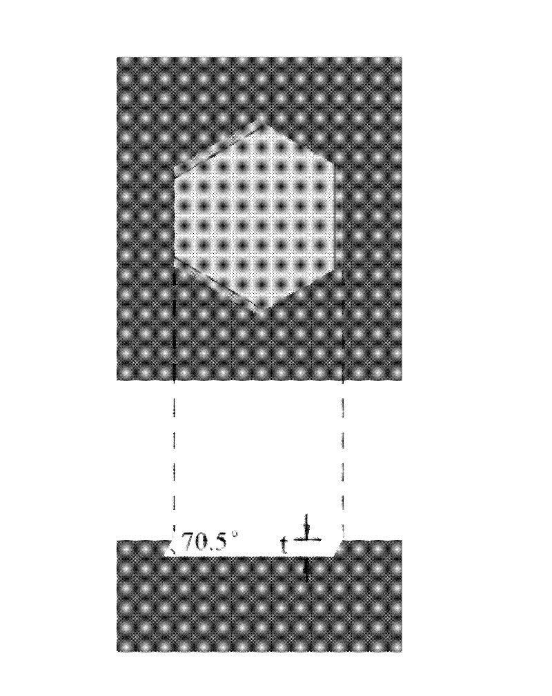
[0034] (111) Design of etching windows on silicon wafers.

[0035] Assume that the x-axis is along the main cutting edge direction of the (111) type silicon wafer, the y-axis is along the crystal direction perpendicular to it, and two identical oblique rectangles are arranged side by side along the x-direction, and the length of the short side of the rectangle is a, The length of the long side of the rectangle is b, the distance between two rectangles is c, and the angle between the short side and the x-axis is α. Under the condition that a, b, and c are all greater than the minimum line width requirement of the mask, two parallel hexagonal etching grooves are formed after anisotropic wet etching of silicon, leaving a wall-shaped single crystal silicon structure in the middle, Its width is d, its length is l, and its inclination angle is 70.5°. When d is on the order of nanometers, a single crystal silicon nanowall structure is formed.

[0036] Preferably, set α=30°, Then...

Embodiment 2

[0041] (111) Process flow for preparing single crystal silicon nanowires on silicon wafer ( Figure 6 ).

[0042] a. Take (111) silicon wafers, after cleaning, high temperature dry oxygen oxidation to form an oxide layer with a thickness of 150nm as a corrosion protection layer;

[0043] b. Design the etching window according to Example 1, get a=6um, b=10.4um, c=3.1um, α=30 °, glue photolithography, BOE (buffer etchant) to remove silicon oxide in the window;

[0044] c.RIE etches the monocrystalline silicon layer to a depth of 500nm, and removes the glue;

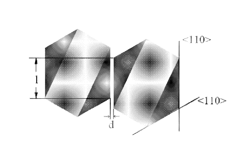
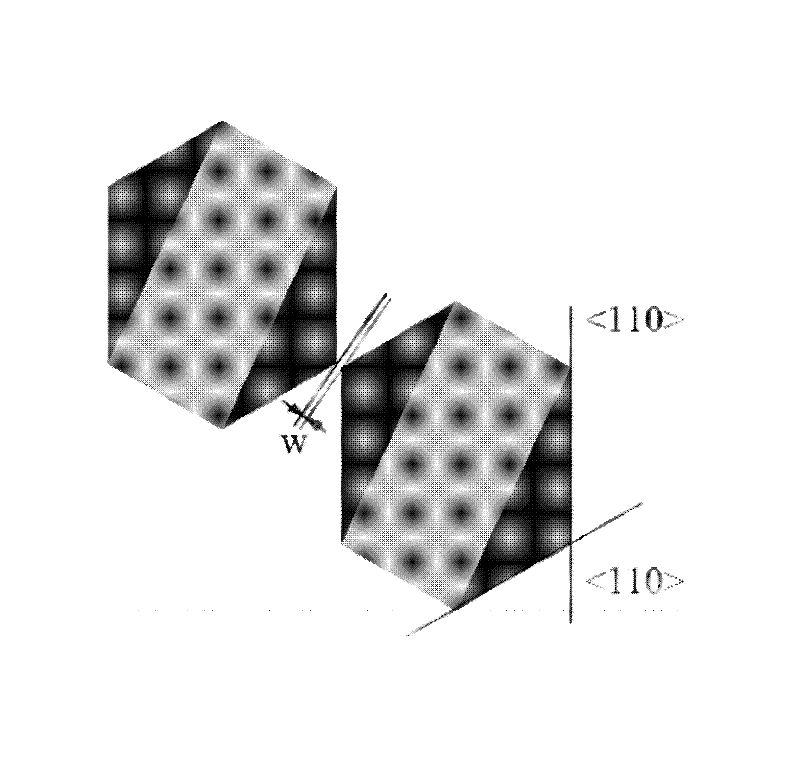
[0045] d. KOH etching, due to the anisotropic wet etching characteristics of (111) silicon wafers, the original two inclined rectangular windows become two hexagonal etching grooves, and a single crystal direction is formed between the two etching grooves. The crystal silicon wall structure has a cross-section of a parallelogram with an inclination angle of 70.5° and a height of about 500nm. The length and width can be d...

Embodiment 3

[0049] A method for preparing single crystal silicon nanostructures on (111) type SOI wafers.

[0050] The method for preparing a single crystal silicon nanostructure on a (111) type SOI sheet is basically the same as the embodiment, the difference is that the height of the nanostructure can be determined by the thickness of the top layer of silicon on the SOI sheet (also including the top layer of silicon that has been thinned by peroxidation in advance). If the thickness is on the order of nanometers, the single crystal silicon nanowall prepared according to the method described in Example 1 also directly forms a nanowire structure.


PUM

PropertyMeasurementUnit
Thicknessaaaaaaaaaa

Abstract

The invention relates to a method for preparing a nano structure on a surface of a (111) silicon wafer, belonging to the technical field of nano. The invention is characterized in that a monocrystalline silicon nano wall structure or nano horn structure of which the characteristic dimension is on a nano level is prepared on the surface of a (111) silicon wafer by utilizing the anisotropic wet-process corrosive characteristic of the silicon material, or a self-restricting oxidation technique is combined to further prepare a monocrystalline silicon nanowire structure of which the cross section is in an inverted triangle shape. The invention has the advantage of simple technique, only relates to conventional photoetching, anisotropic wet-process etching mask manufacturing, corroding and etching techniques, can implement large-scale manufacture, and is a convenient micro/nano integration technology. The nano structure manufactured by the method provided by the invention can be used for researching properties (including mechanical, thermal, electric and other properties) of a low-dimension monocrystalline silicon material structure, can be used as a functional structure component of a sensor, and has application prospects.

Description

technical field [0001] The invention relates to a method for preparing a single crystal silicon nanostructure from top to bottom, more precisely, the invention relates to a method for preparing a nanostructure on the surface of a (111) type silicon chip, which belongs to the field of nanotechnology. Background technique [0002] With the development of nanoscience and technology, the nanostructure of materials has been paid more and more attention by researchers because they often show different characteristics from their macroscopic states. Research, so as to better understand various effects at the nanoscale, achieve a deeper understanding of the relationship between the microstructure of materials and their properties, and thus design and manufacture application devices with better performance. [0003] At present, there are two types of methods for preparing nanowires, the first is the bottom-up method (bottom-up) (Xia Y., Yang P., Sun Y., W, Y., Mayers B., Gates B. , Y...

Claims


Application Information

Patent Timeline
IPC IPC(8): H01L21/02C30B33/08B82Y40/00
Inventor 金钦华俞骁李铁王跃林
Owner SHANGHAI INST OF MICROSYSTEM & INFORMATION TECH CHINESE ACAD OF SCI
Why Eureka
Try Eureka