

Manufacturing method of mechanical uniaxial strain GeOI (germanium-on-insulator) wafer based on SiN buried insulating layer
A uniaxial strain and manufacturing method technology, applied in the field of microelectronics, can solve the problems of easily broken silicon wafers, complex process steps, long manufacturing cycle, etc., and achieve the effects of low manufacturing cost, simple manufacturing process and less equipment
- Summary
- Abstract
- Description
- Claims
- Application Information
AI Technical Summary
Problems solved by technology
Method used
Image

Examples
Embodiment 1
[0035] Example 1: Preparation of 3-inch Uniaxially Strained GeOI Wafers
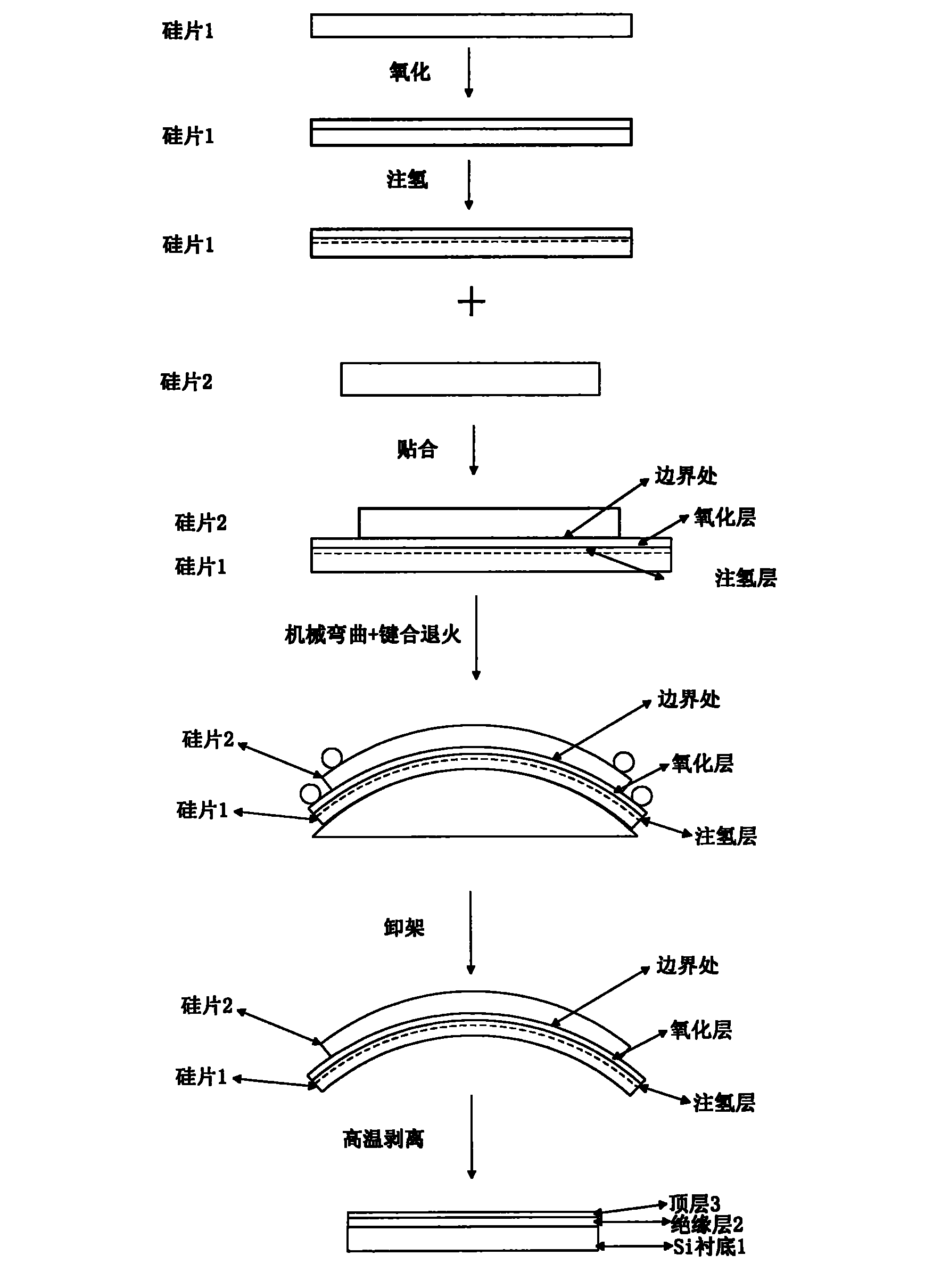
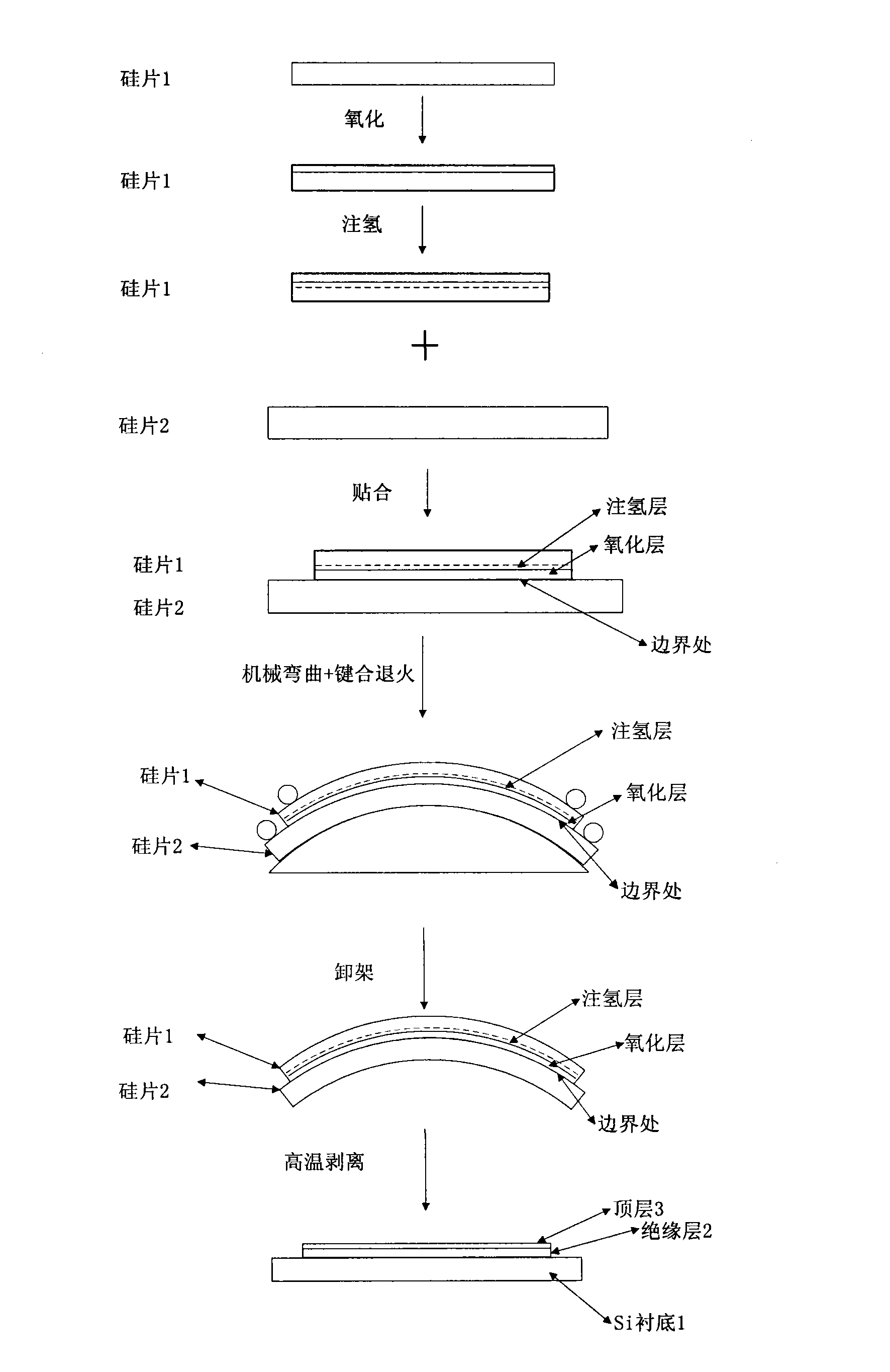
[0036] 1. GeOI wafer selection: 3-inch (100) or (110) wafer ((100) or (110) refers to a certain crystal surface of the GeOI wafer crystal surface), Si substrate thickness 0.4mm, The SiN buried insulating layer is 500nm thick, and the top layer Si is 500nm thick.
[0037] GeOI wafer diameter selection: The larger the diameter of the GeOI wafer, the smaller the minimum bending radius of its bending, and the greater the strain amount of the obtained uniaxially strained GeOI wafer, and the electron migration of the final uniaxially strained GeOI wafer. The higher the rate and hole mobility enhancement is. For the uniaxial strained GeOI wafer based on the SiN buried insulating layer produced by the present invention, GeOI wafers with different diameters from 3 inches to 8 inches can be selected according to the different processes of the GeOI devices and circuits.
[0038] GeOI wafer crystal plane and cryst...
Embodiment 2
[0056] Example 2: Preparation of 4-inch Uniaxial Strained GeOI Wafers
[0057] 1. GeOI wafer selection: 4 inches (100) or (110) crystal plane, Si substrate thickness 0.55mm, SiN buried insulating layer thickness 300nm, top Ge layer thickness 50nm.
[0058] 2. Selection of bending radius of curvature: According to the selected GeOI wafer, the radius of curvature of the bending table is selected to be 0.75m.
[0059] 3. GeOI wafer bending process steps:
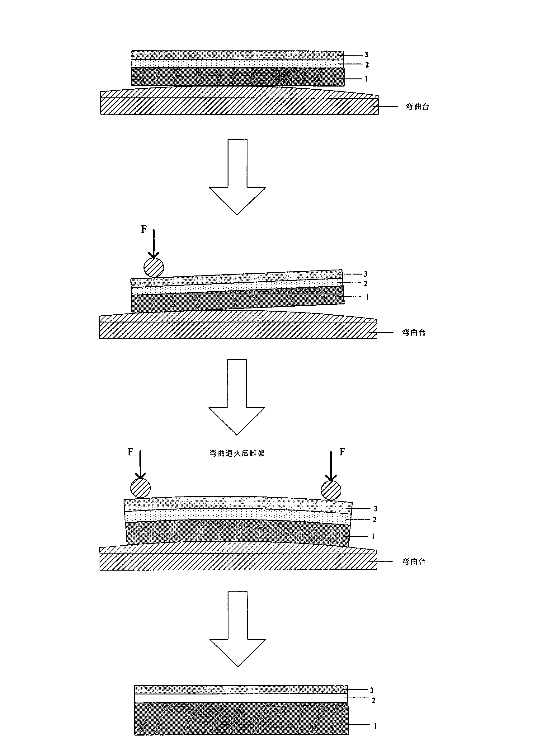
[0060] 1) Place the top Ge layer of the GeOI wafer up (or down) on a clean stainless steel curved bending table with its or direction parallel to the bending direction, such as image 3 or Figure 4 shown;
[0061] 2) The two cylindrical horizontal pressing rods on the bending table are placed horizontally at both ends of the GeOI wafer, 1 cm away from the edge;
[0062] 3) Rotate the top rod nut of one of the pressing rods on the bending table to fix one end of the GeOI wafer first;
[0063] 4) Slowly rotate the top pin...
Embodiment 3
[0071] Example 3: Preparation of 6-inch Uniaxially Strained GeOI Wafers
[0072] 1. GeOI wafer selection: 6 inches (100) or (110) crystal plane, Si substrate thickness 0.68mm, SiN buried insulating layer thickness 1000nm, top layer SiGe thickness 1000nm.
[0073] 2. Selection of bending radius of curvature: According to the selected GeOI wafer, the radius of curvature of the bending table is selected to be 0.5m.
[0074] 3. GeOI wafer bending process steps:
[0075] 1) Place the top layer of the GeOI wafer SiGe face up (or down) on the curved bending table, and its bending direction is parallel to the or direction, such as image 3 or Figure 4 shown;
[0076] 2) The two cylindrical horizontal pressing rods on the bending table are placed horizontally at both ends of the GeOI wafer, 1 cm away from the edge;
[0077] 3) Rotate the top rod nut of one of the pressing rods on the bending table to fix one end of the GeOI wafer first;
[0078] 4) Slowly rotate the top pin nut...
PUM
 Abstract
Description
Claims
Application Information