Method for millimeter-sized micro nanostructure nano carving and processing through adopting antifrictional metal (AFM) needle

A technology of micro-nano structure and micro-structure, applied in the directions of micro-structure technology, micro-structure device, manufacturing micro-structure device, etc., can solve problems such as the limitation of scanning range of scanning ceramic tubes, and achieve the integration of processing and detection, the method is simple, and the equipment And the effect of low processing cost

Inactive Publication Date: 2012-07-04
HARBIN INST OF TECH
View PDF3 Cites 22 Cited by
  • Summary
  • Abstract
  • Description
  • Claims
  • Application Information

AI Technical Summary

Problems solved by technology

However, the biggest problem with this method at present is: limited by the scanning range of the scanning ceramic tube, its processing range is

Method used


Image

  • Method for millimeter-sized micro nanostructure nano carving and processing through adopting antifrictional metal (AFM) needle
  • Method for millimeter-sized micro nanostructure nano carving and processing through adopting antifrictional metal (AFM) needle
  • Method for millimeter-sized micro nanostructure nano carving and processing through adopting antifrictional metal (AFM) needle

Examples


specific Embodiment approach 1

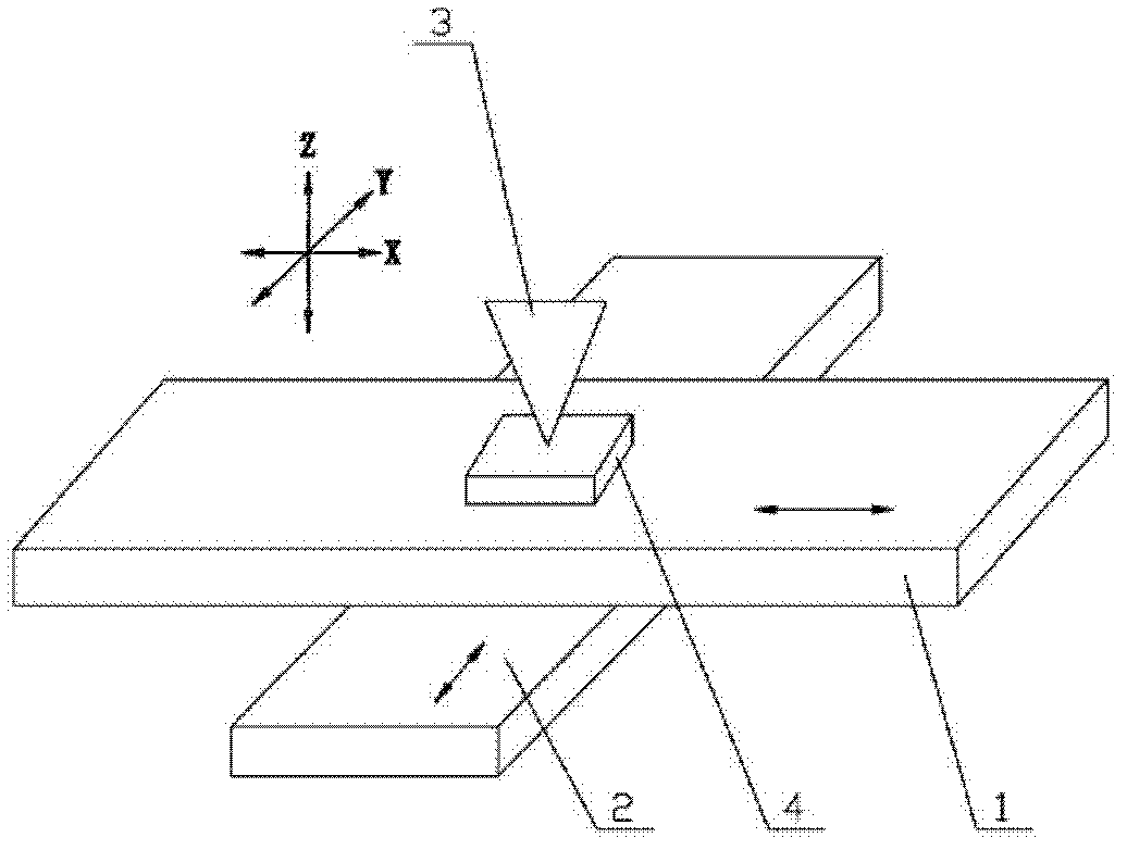
[0023] Specific implementation mode one: as Figure 1a ~ Figure 1c and Figure 3b , a method for processing millimeter-sized micro-nano structures using AFM probe nanometer scribing, the method is implemented by the following steps:

[0024] Step 1: first place the sample 4 to be processed on the X-Y two-dimensional precision workbench, and determine the starting point of the structure to be processed of the sample 4 to be processed within the range of length × width = 100mm × 100mm through the X-Y two-dimensional precision workbench; then pass The approach process of the AFM system makes the AFM probe 3 contact the surface of the sample 4 to be processed with a vertical load less than 1 μN;

[0025] Step 2: Process the nanowire vibrating structure; first set the scanning range of the AFM to 0 μm, and then set the parameter values ​​of the processing length, processing width, processing distance, processing direction, vertical load and processing speed, and the above-mentione...

specific Embodiment approach 2

[0027] Specific implementation mode two: as Figure 1a ~ Figure 1c and Figure 3c , a method for processing millimeter-sized micro-nano structures using AFM probe nanometer scribing, the method is implemented by the following steps:

[0028] Step 1: first place the sample 4 to be processed on the X-Y two-dimensional precision workbench, and determine the starting point of the structure to be processed of the sample 4 to be processed within the range of length × width = 100mm × 100mm through the X-Y two-dimensional precision workbench; then pass The approach process of the AFM system makes the AFM probe 3 contact the surface of the sample 4 to be processed with a vertical load less than 1 μN;

[0029] Step 2: Processing an array microstructure composed of multiple identical single microstructures; the shape of a single microstructure is circular, square or equilateral triangle, the diameter of a single circular microstructure is 5 μm-50 μm, and a single The side length of the...

Embodiment 1

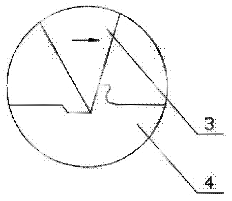
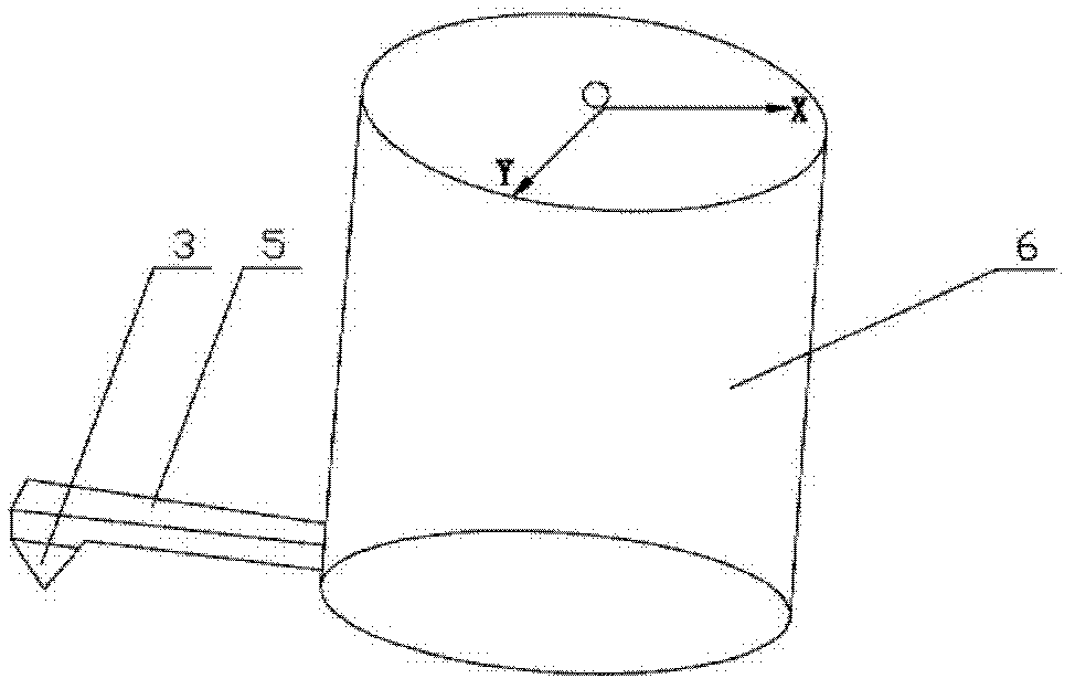
[0031]Embodiment 1: Taking the realization process of machining an equilateral triangle microstructure on the surface of a sample to be processed as an example to describe the realization of the coordinate acquisition and movement of a single microstructure: using the Ambios Qscope 250 of Quesant Instrument Corporation of the United States TM The V4.05 version software of the AFM system, the software provides the Slew_xy(x, y) function to control the precise movement of the AFM scanning ceramic tube 6 to drive the AFM probe 3, and this function controls the movement of the AFM probe to the (x, y) coordinates place. Therefore, as long as the figure 2 The start and end coordinates of each line shown in the figure can realize the movement of the AFM probe 3 by calling the Slew_xy function to complete the processing, such as Figure 1a ~ Figure 1c .

[0032] The process of obtaining coordinates: such as figure 2 As shown, when the equilateral triangle microstructure is proce...


PUM

PropertyMeasurementUnit
Diameteraaaaaaaaaa
Center distanceaaaaaaaaaa
Diameteraaaaaaaaaa

Abstract

The invention discloses a method for millimeter-sized micro nanostructure nano carving and processing through adopting an antifrictional metal (AFM) needle, which belongs to the field of millimeter-sized micro nanostructure processing. The method can solve the processing problem of a millimeter-sized and nano-precision micro nanostructure under lower cost. The method 1 is that: a sample to be processed is firstly placed on an X-Y two-dimensional precision workbench, and the AFM needle is contacted with the surface of the sample which is to be processed and has the vertical load smaller than 1muN through the approaching process of an AFM system; and a nano linear array structure is processed, and the parameter values of the processing length, the processing width, the processing space, the processing direction, the vertical load and the processing speed are set. The method 2 is different from the method 1 is that: an array microstructure which is formed by combining a plurality of same microstructures is processed; and firstly, the processing parameter is set, during the processing, a scanning earthenware pipe drives the AFM needle to move, and accordingly, square, round or equilateral triangular array microstructures are processed. The method adopts the AFM needle for the millimeter-sized micro nanostructure nano carving and processing of the sample to be processed.

Description

technical field [0001] The invention belongs to the field of processing millimeter-sized micro-nano structures, in particular to a method for processing millimeter-sized micro-nano structures based on AFM probe nanometer scribing. Background technique [0002] Complex microstructures with nanometer precision have a wide demand in many fields, such as high-density grating structures, complex three-dimensional micro-nano structures, etc., have been widely used in binary micro-optics, X-ray astronomical telescopes, extreme ultraviolet lithography, laser inertial confinement Nuclear fusion diagnostic system, experimental mechanics, surface engineering and many other fields. For the above-mentioned structures, the processing methods currently used are mainly traditional nano-processing methods such as electron beam processing, focused ion beam, and laser processing. However, expensive processing equipment, harsh processing conditions, micron-sized processing range, and low proces...

Claims


Application Information

Patent Timeline
IPC IPC(8): B81C1/00
Inventor 闫永达赵学森胡振江魏盈盈高大为孙涛董申
Owner HARBIN INST OF TECH
Why Eureka
Try Eureka