Metal interconnection structure and manufacturing method thereof

A metal interconnection structure and manufacturing method technology, applied in radiation control devices, semiconductor/solid-state device manufacturing, electrical components, etc., can solve problems such as color mixing and affecting imaging quality, reduce crosstalk, improve K value, The effect of easy detection

Active Publication Date: 2012-07-04
GALAXYCORE SHANGHAI
View PDF2 Cites 1 Cited by
  • Summary
  • Abstract
  • Description
  • Claims
  • Application Information

AI Technical Summary

Problems solved by technology

In addition, for color CMOS image sensors, optical crosstalk will cause color mixing problems

Method used


Image

  • Metal interconnection structure and manufacturing method thereof
  • Metal interconnection structure and manufacturing method thereof
  • Metal interconnection structure and manufacturing method thereof

Examples


Embodiment 1

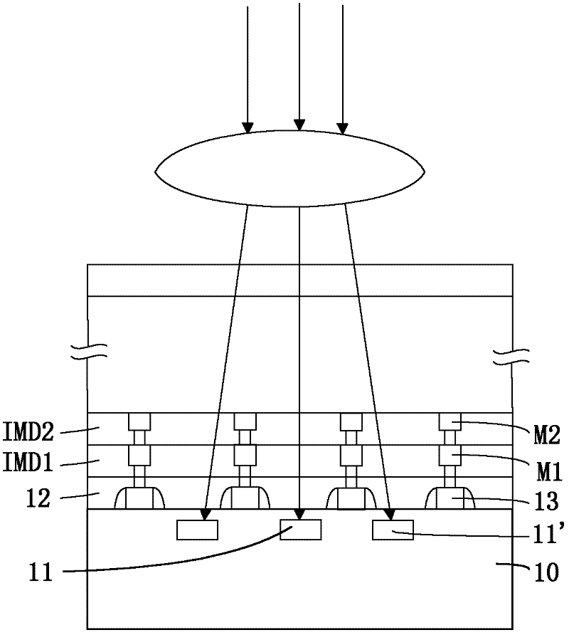
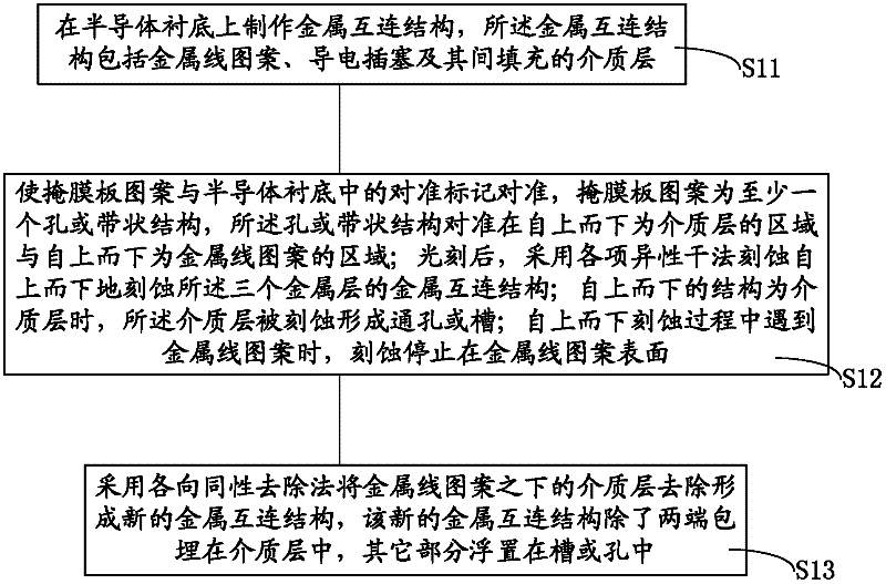
[0063] Taking the image sensor as an example, the metal interconnection structure and the manufacturing method therein will be introduced in detail below. figure 2 It is a flow chart of the method for fabricating the metal interconnection structure provided in the first embodiment. Figure 3 to Figure 6 It is a schematic diagram of the intermediate structure during the fabrication process of the metal interconnection structure. Figure 7 The completed top view for the metal interconnect structure, Figure 8 , Figure 9 respectively Figure 7 The cross-sectional view along the A-A line and the B-B line.

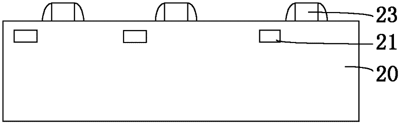
[0064] combine figure 2 , Figure 8 and Figure 9 , S11 is firstly performed to fabricate a metal interconnection structure 27 on the semiconductor substrate 20, the metal interconnection structure 27 including a metal line pattern, a conductive plug and a dielectric layer filled therebetween.

[0065] Specifically, in combination with the image sensor, the execution ...

Embodiment 2

[0098] During the execution of step S12, except that the hole or band structure in the mask pattern provided in the photolithography process of the first embodiment is aligned between the area of ​​the dielectric layer from top to bottom and the metal line pattern from top to bottom Outside the region, the holes or band-shaped structures in the mask pattern provided in the photolithography process of the second embodiment are only aligned in the region of the dielectric layer from top to bottom, and the mask pattern is transferred to the photoresist After being put on, a strip-shaped exposure area 28' is formed, and its top view is as follows Figure 17 shown. Using the photoresist pattern as a mask, in the top-down etching process, only the dielectric layer is encountered, and the dielectric layer is etched to form through holes or grooves, and the cross-sectional view of the formed structure along the B-B line is as follows Figure 18 shown. The parameters used in the etch...


PUM


Abstract

The invention provides a metal interconnection structure and a manufacturing method thereof. The manufacturing method comprises the following steps of: manufacturing a metal interconnection structure on a substrate, wherein the metal interconnection structure comprises a metal wire pattern, a conductive plug and a medium layer which is filled between the metal wire pattern and the conductive plug; performing photoetching, and etching the metal interconnection structure by adopting an anisotropic dry etching method from top to bottom, and at least forming a through hole or a groove on an area which is a medium layer from top to bottom; and removing the medium layer below the metal wire pattern by adopting an isotropic removing method to form a novel metal interconnection structure, wherein the two ends of the novel metal interconnection structure are embedded into the medium layer, and other parts of the novel metal interconnection structure float in the groove or the hole. Due to the adoption of the technical scheme of the invention, certain requirements on a suspended metal interconnection structure can be met, e.g., non-matching conditions with a lens can be reduced, the light crosstalk phenomenon is reduced, and needed materials can be filled into a suspended structure.

Description

technical field [0001] The invention relates to the field of semiconductor manufacturing, in particular to a metal interconnection structure and a manufacturing method thereof. Background technique [0002] Currently, image sensors entering the market are classified into complementary metal oxide semiconductor (Complementary Metal Oxide Semiconductor, CMOS) sensors and charge-coupled device (Charge-coupled Device, CCD) sensors. CMOS or CCD sensors usually have hundreds of thousands or even millions of pixels to convert light signals into electrical signals, so that the original images of people or objects are converted into electrical signals in the image sensor. CMOS or CCD image sensors have been widely used in various digital image devices, such as digital cameras, digital video cameras and other electronic devices, due to their advantages of small size, low power consumption, and low cost. [0003] Regarding the structure of the CMOS image sensor in the prior art, such ...

Claims


Application Information

Patent Timeline
IPC IPC(8): H01L21/768H01L27/146H01L23/528
Inventor 赵立新李文强李杰蒋珂玮
Owner GALAXYCORE SHANGHAI
Why Eureka
Try Eureka