Multiple-quantum well waveguide butt-coupling method

A docking coupling and multi-quantum well technology, which is applied in the field of multi-quantum well waveguide docking coupling, can solve the problems of difficult precise control of corrosion depth, inconsistent corrosion depth, and low coupling efficiency, so as to avoid insertion loss, improve the quality of docking coupling, and improve The effect of material quality

Active Publication Date: 2012-07-04
WUHAN HUAGONG GENUINE OPTICS TECH
View PDF3 Cites 14 Cited by
  • Summary
  • Abstract
  • Description
  • Claims
  • Application Information

AI Technical Summary

Problems solved by technology

Although the ideal interfacial corrosion morphology can be obtained by using non-selective etching solution, it is difficult to accurately control the corrosion depth, and the process repeatability is poor; on the other hand, using selective etching solution, although the corrosion depth can be very good Control, but the lateral corrosion depth of different materials is inconsistent, which will easily lead to voids at the interface during butt coupling growth, and the coupling efficiency is not high

Method used


Image

  • Multiple-quantum well waveguide butt-coupling method
  • Multiple-quantum well waveguide butt-coupling method
  • Multiple-quantum well waveguide butt-coupling method

Examples


Embodiment Construction

[0044] The method of the present invention will be further described in detail below in conjunction with the accompanying drawings and embodiments of the present invention.

[0045] The main idea of ​​the present invention is to use non-selective corrosion to control the interface corrosion morphology, and use selective corrosion to accurately control the corrosion depth, and use metal organic chemical vapor deposition (MOCVD) high temperature heat treatment method to optimize the interface corrosion morphology, Therefore, the light loss at the docking interface is small, and the process is simple and repeatable.

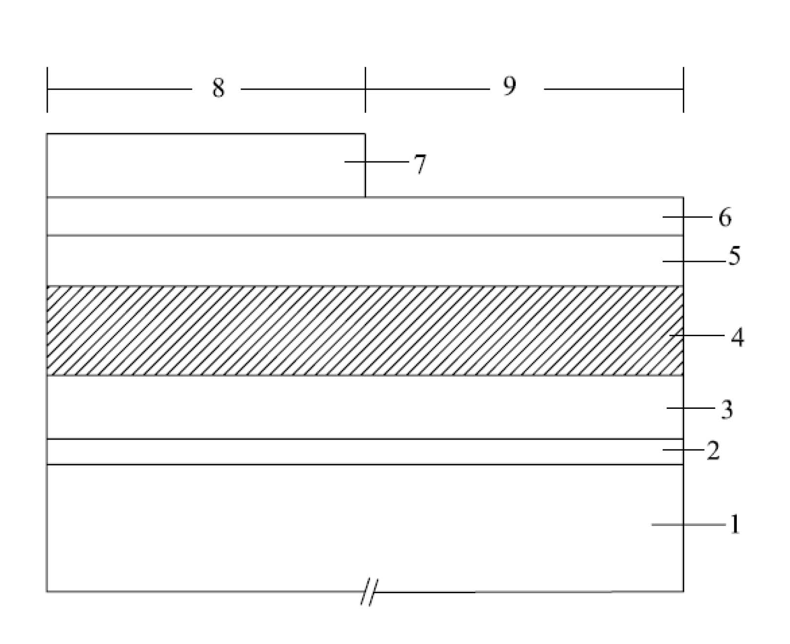
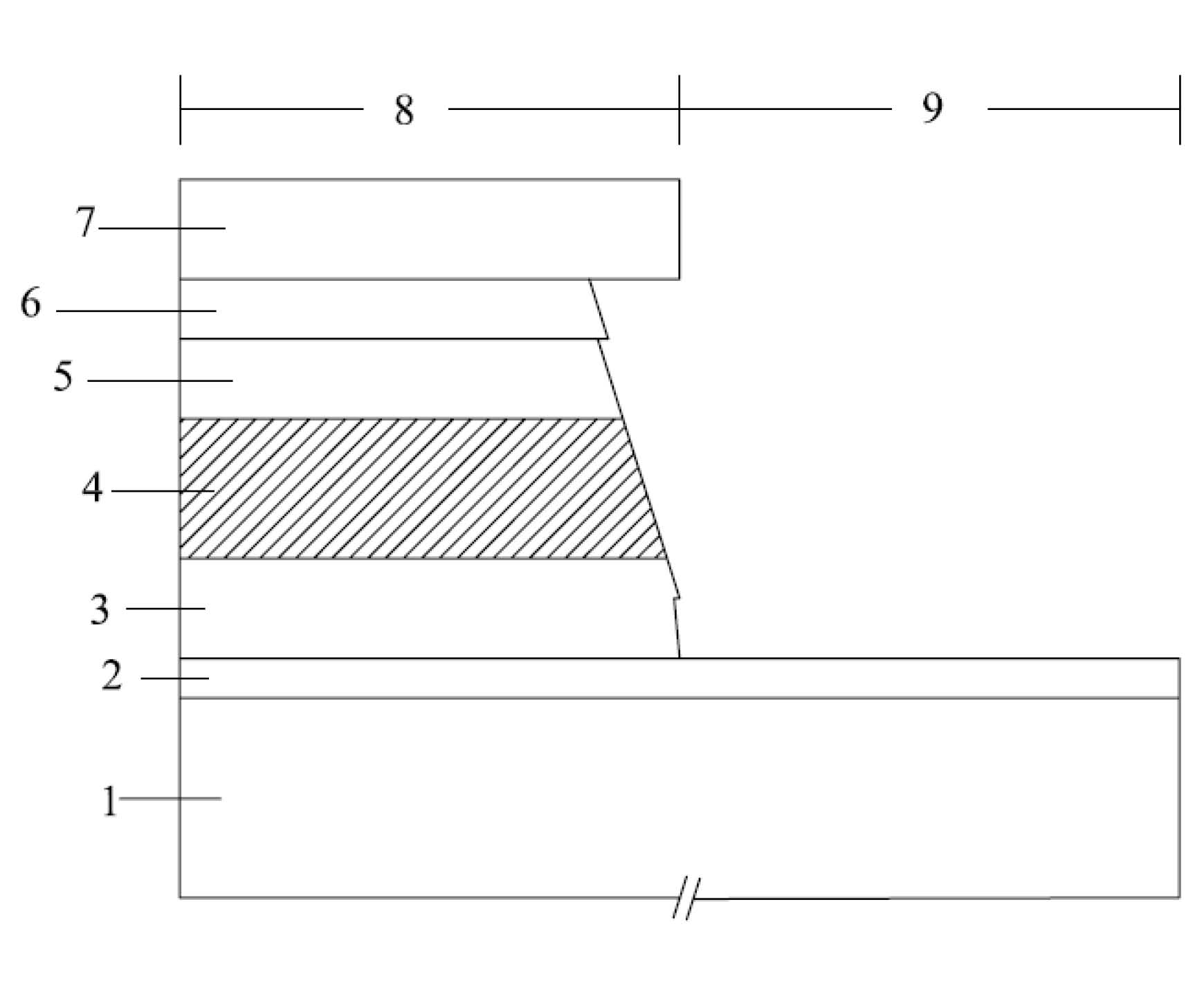
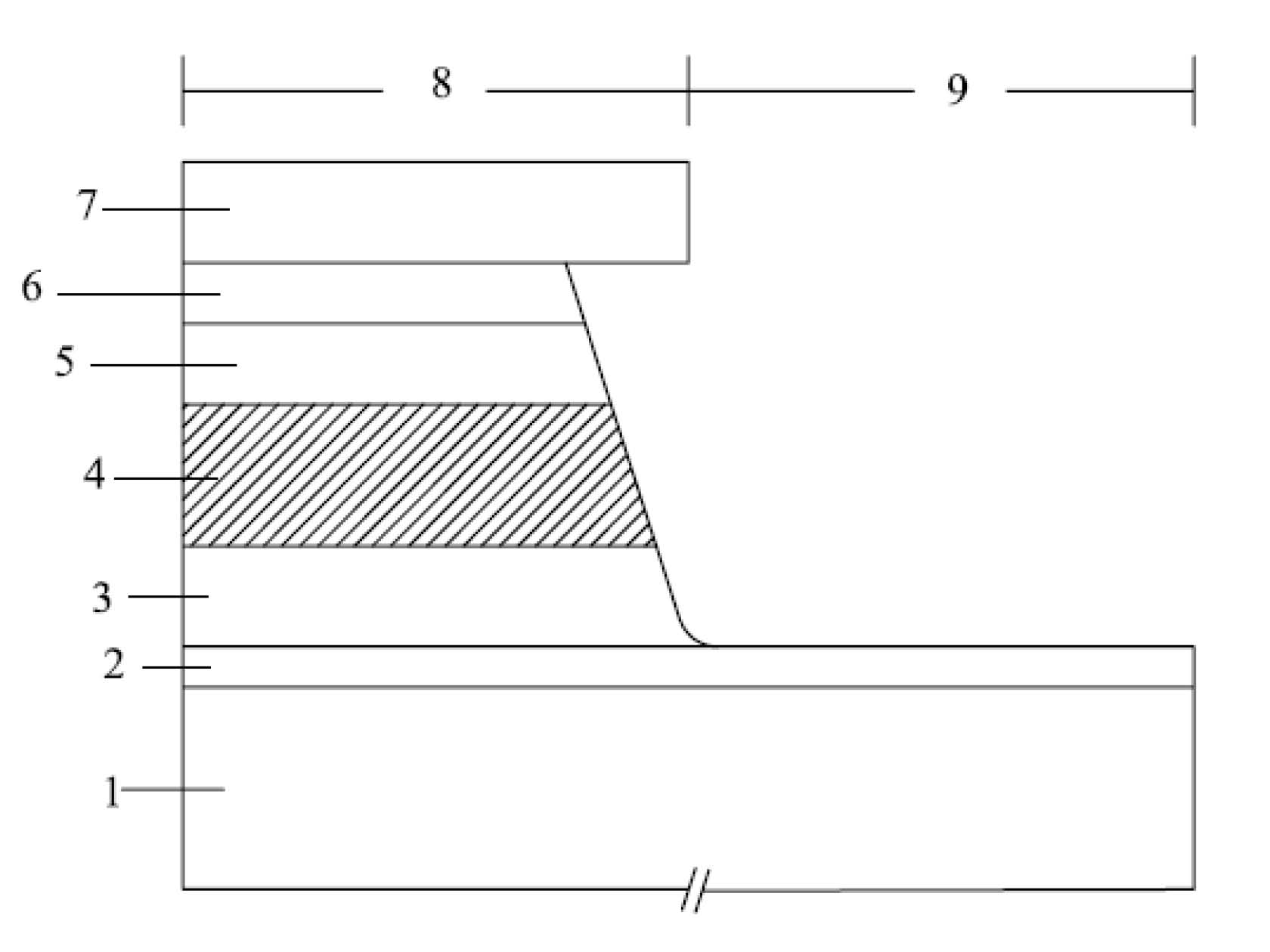
[0046] figure 1 It is a schematic diagram of a single-epitaxial multi-quantum well structure of the present invention, referring to Figure 2 ~ Figure 4 , the multi-quantum well waveguide butt coupling method mainly includes the following steps:

[0047] Step 1: Epitaxially epitaxially first the first multiple quantum well structure on the N-type substrate.

[00...


PUM


Abstract

The invention relates to a multiple-quantum well waveguide butt-coupling method comprising the following steps of: A, carrying out primary epitaxy on a substrate to obtain a multiple-quantum well structure; B, after a dielectric film is deposited, carrying out mask photoetching, and removing a waveguide part of a first region requiring secondary epitaxy by using a three-step etching method; C, placing an epitaxial wafer into metal organic chemical vapor deposition equipment for high-temperature treatment; and D, carrying out secondary epitaxial growth to obtain a second multiple-quantum well structure. By using the method, an attractive interface etching appearance can be achieved, cavities caused during growth can be avoided, the butting quality can be effectively improved, the coupling loss can be reduced, and good repeatability can be obtained. The multiple-quantum well waveguide butt-coupling method can be used for manufacture and batch production of various photoelectronic integrated chips.

Description

technical field [0001] The invention relates to optoelectronic device integration technology, in particular to a multi-quantum well waveguide butt coupling method, which is used in the manufacturing process of semiconductor optoelectronic integrated chips. Background technique [0002] At present, a large number of discrete devices are used in optical fiber communication systems. These discrete devices not only need to be individually packaged, but also need to be precisely coupled and aligned with the input / output optical fiber. The coupling and alignment of the device and the optical fiber is not only time-consuming, but also often due to The mismatch between the fiber mode field and the device mode field leads to a huge coupling loss. At the same time, the existence of a large number of input / output fiber and device coupling connection points will also bring hidden dangers to reliability, and independent device packaging also leads to increased costs. [0003] Monolithic...

Claims


Application Information

Patent Timeline
Patent Type & Authority Applications(China)
IPC IPC(8): H01S5/20H01S5/34
Inventor 周志强刘建军唐琦
Owner WUHAN HUAGONG GENUINE OPTICS TECH
Why Eureka
Try Eureka