Gas and pressure composite sensor and preparation method thereof
A composite sensor and pressure technology, applied in the direction of instruments, measuring devices, etc., can solve the problems of difficult temperature control, difficult to popularize and apply, increase chip power, etc., to avoid pressure measurement errors, reduce chip occupation area, and avoid measurement errors Effect
- Summary
- Abstract
- Description
- Claims
- Application Information
AI Technical Summary
Problems solved by technology
Method used
Image
Examples
preparation example Construction
[0067] The present invention also discloses a method for preparing the above-mentioned gas and pressure composite sensor, comprising the steps of:
[0068] Perform P-type doping on the substrate (such as silicon wafer 1) to form a P-type doped region;
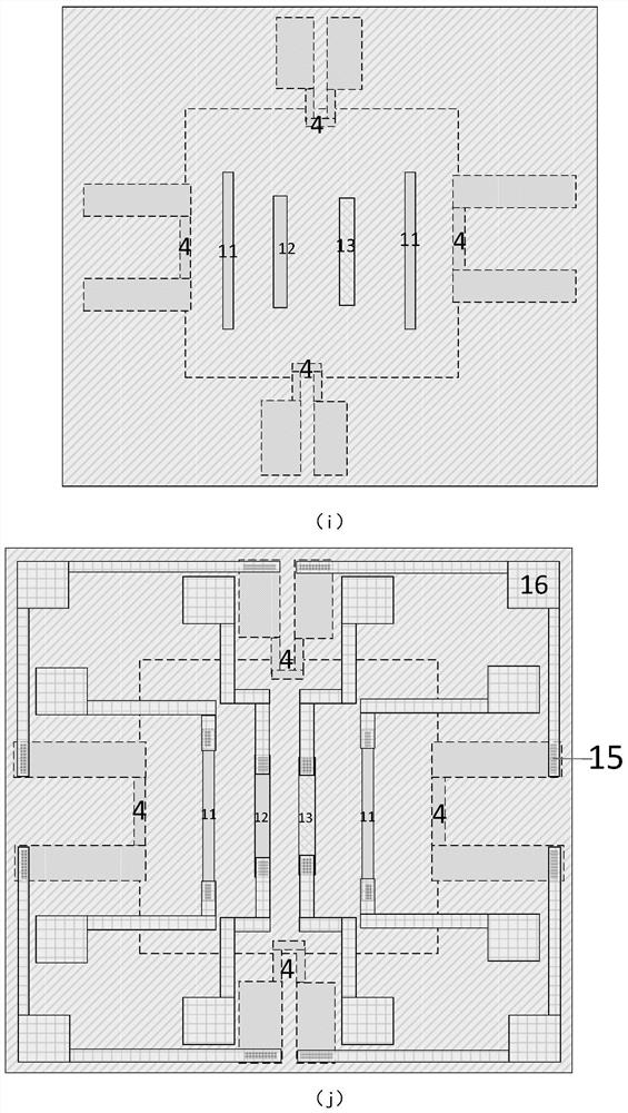
[0069] Deposit a gas sensitive resistor 13, a temperature measuring resistor 12 and a heating resistor 11 on a predetermined area on the front side of the silicon wafer 1, and deposit interconnection lines and pads 16;
[0070] Etching is performed on the back side of the silicon wafer 1 to form a strain chamber 8, and the position of the strain chamber 8 corresponds to a predetermined area on the front side of the silicon wafer 1;
[0071] The back side of the silicon wafer 1 and the bonding wafer 17 are anodically bonded in a vacuum environment to form a vacuum strain chamber 8 to obtain a final gas and pressure composite chip.
[0072] In a specific embodiment, the preparation of the gas sensitive resistor 13, the temperatu...
Embodiment 1
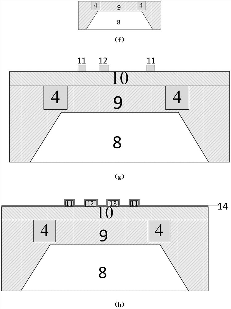
[0077] The preparation method of the air pressure composite sensor (abbreviation, gas and pressure composite sensor) of this embodiment, its preparation process flow chart is as follows figure 1 shown, including the following steps:
[0078] (1) On the surface of N(100) double parabolic silicon wafer 1, oxidize and grow implanted buffer protection layer 2, such as figure 1 As shown in (a), specifically: grow a silicon dioxide film on the surface of a silicon wafer by thermal oxidation, with a thickness of 50-500 Å; of course, dry oxidation, wet oxidation or CVD can also be used to prepare a silicon dioxide film. Silicon oxide film;
[0079] (2) The surface of the buffer protective layer 2 obtained in step (1) is subjected to photolithography and development to prepare the first implantation of the first barrier layer 3, exposing areas such as varistors, interconnection lines and pads 16, and using ion P-type doping is performed on regions such as top-layer varistors, interco...
Embodiment 2
[0092] The preparation method of the gas and pressure composite sensor of this embodiment, its preparation process is as follows Figure 5 shown, including the following steps:
[0093] 1) On the surface of the P(100) double-polished SOI sheet 18, oxidize and grow and inject the buffer protection layer 2, such as Figure 5 As shown in (a), specifically: grow a silicon dioxide film on the surface of the SOI sheet 18 by thermal oxidation, with a thickness of 50A-500A;
[0094] 2) In step 1), the front side of the SOI sheet 18 on which the implanted buffer protection layer 2 has been grown is subjected to ion implantation doping and annealing to form a P-type doped region 4, such as Figure 5 As shown in (b), the doping concentration of the P-type doped region 4 after annealing is 3×10 18 cm -3 ~3×10 20 cm -3 ;P-type substrate doping concentration is lower than 2×10 18 cm -3 ;
[0095] 3) Prepare the piezoresistive etching second barrier layer 20 by uniform photolithograp...
PUM
 Abstract
Description
Claims
Application Information


