Method for preparing two-sided silicon nano-wire array

A silicon nanowire array, double-sided technology, applied in the field of preparation of double-sided silicon nanowire arrays

Inactive Publication Date: 2012-07-11
JIANGSU UNIV
View PDF5 Cites 12 Cited by
  • Summary
  • Abstract
  • Description
  • Claims
  • Application Information

AI Technical Summary

Problems solved by technology

The Bottom-Up method and the dry etching bulk silicon surface method usually need to be prepared under high temperature conditions using relatively sophisticated and expensive equipment. These factors lead to a significant increase in the preparation cost of silicon nanowire arrays, and at the same time, the preparation efficiency is also low. It is not too high, so it is difficult to achieve a wide range of industrial applications; this paper proposes a method of wet etching silicon surface to prepare silicon nanowire arrays, the schematic diagram of which is shown in Figure 1 shows that this method is prepared at a lower temperature by using the corrosiveness of the solution, and has the advantages of simple operation and no equipment The advantages of demand and easy control

Method used


Image

  • Method for preparing two-sided silicon nano-wire array
  • Method for preparing two-sided silicon nano-wire array
  • Method for preparing two-sided silicon nano-wire array

Examples


Embodiment 1

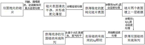
[0024] 1. Silicon wafer cleaning:

[0025] Wash with acetone and alcohol ultrasonic vibration respectively, room temperature for 10 min;

[0026] into concentrated H 2 SO 4 :H 2 o 2 =3:1 (V:V) solution boiled for 30 min;

[0027] Rinse the glass surface with deionized water;

[0028] Blow dry with high-purity nitrogen.

[0029] 2. Put the cleaned silicon wafer into 5% HF acid solution and corrode for 3 min at room temperature.

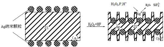
[0030] 3. Put the silicon wafer into HF acid and AgNO quickly at room temperature 3 The mixed solution, which contains 3mol of HF acid per liter of mixed solution, contains AgNO per liter of mixed solution 3 0.01 mol, and stirred slowly for 40 s, and then the surface of the silicon wafer was washed repeatedly with deionized water.

[0031] 4. Pad and fix the silicon wafer, put it into HF acid and H 2 o 2 The mixed solution of the composition was treated for 40min, wherein every liter of mixed solution contained 2.8 mol of HF acid, and every ...

Embodiment 2

[0034] 1, step 1 is the same as embodiment 1.

[0035] 2, step 2 is the same as embodiment 2.

[0036] 3. HF acid and AgNO in step 3 3 The mixed solution, wherein every liter of mixed solution contains HF acid is 4.8mol, and every liter of mixed solution contains AgNO 3 0.05 mol and stirred slowly for 30 s.

[0037] 4. Put HF acid and H in step 4 2 o 2 The mixed solution of the composition was treated for 30min, wherein every liter of mixed solution contained 4.8 mol of HF acid, and every liter of mixed solution contained H 2 o 2 The solution is 0.15mol.

[0038] 5. Step 5 is the same as Step 5 in Example 1.

Embodiment 3

[0040] 1, step 1 is the same as embodiment 1.

[0041] 2, step 2 is the same as embodiment 2.

[0042] 3. HF acid and AgNO in step 3 3 The mixed solution, which contains 3.6mol of HF acid per liter of mixed solution, contains AgNO per liter of mixed solution 3 0.03 mol and stirred slowly for 90 s.

[0043] 4. Put HF acid and H in step 4 2 o 2 The mixed solution of the composition was treated for 60 minutes, wherein each liter of mixed solution contained 3.2 mol of HF acid, and each liter of mixed solution contained H 2 o 2 The solution is 0.4mol.

[0044] 5. Step 5 is the same as Step 5 in Example 1.

[0045] The silicon nanowires prepared by the present invention have a length of 2 to 3 microns and a diameter of 50 to 100 nanometers; the density of the silicon nanowires on the silicon chip surface reaches 10 4 ~10 5 roots per square centimeter.


PUM

PropertyMeasurementUnit
lengthaaaaaaaaaa
diameteraaaaaaaaaa

Abstract

The invention relates to a silicon nano-wire, in particular to a method for preparing a two-sided silicon nano-wire array. According to the method, a silicon surface is etched by combining the corrosivity of a solution and the catalysis of metal ions at low temperature to form the silicon nano-wire array. The method comprises the following steps of: cleaning the silicon surface; passivating the surface of a silicon wafer by using hydrogen; covering a uniform layer of silver nanoparticle network on each of two surfaces of the silicon wafer by using a chemical plating method; preparing the two-sided silicon nano-wire array; and removing excessive silver nanoparticles. The method has the advantages that: expensive equipment and high-temperature environment are avoided in the preparation process, and the method is easy to operate and control, low in cost and high in efficiency, and can be applied to large-scale industrial production.

Description

technical field [0001] The invention relates to silicon nanowires, in particular to a method for preparing a double-sided silicon nanowire array. Background technique [0002] Silicon nanowires have many novel physical properties that are significantly different from other low-dimensional semiconductor materials, such as electricity, optics, magnetism, and mechanics, which make them ideal for field-effect devices, single-electron storage devices, photodetection devices, nanosensors, and high-efficiency light-emitting devices. It has potential applications in solar cells, especially in improving solar cell light absorption, spectral response, effective electron-hole separation and anti-reflection, etc., so the research of one-dimensional silicon nanowires has received great attention; The preparation methods of nanowire arrays include Bottom-Up method and Top-Down method, wherein the Bottom-Up method is mainly based on Fe, Au, Ni, Ti, SiO x etc. as catalysts or directly usi...

Claims


Application Information

Patent Timeline
Patent Type & Authority Applications(China)
IPC IPC(8): B81C1/00
Inventor 丁建宁张福庆郭立强程广贵凌智勇张忠强杨娟孙东健
Owner JIANGSU UNIV
Why Eureka
Try Eureka