Inner electrode of glass-ceramic stacked capacitor and preparation method of the inner electrode

A technology of laminated capacitors and glass ceramics, applied in the direction of laminated capacitors, fixed capacitor electrodes, fixed capacitor dielectrics, etc., can solve the problems of reduced effective area of ​​internal electrodes, expensive preparation costs, and restrictions on the application environment of capacitors, etc.

Inactive Publication Date: 2012-07-11
GENERAL RESEARCH INSTITUTE FOR NONFERROUS METALS BEIJNG
View PDF4 Cites 7 Cited by
  • Summary
  • Abstract
  • Description
  • Claims
  • Application Information

AI Technical Summary

Problems solved by technology

Under normal technology, the internal electrodes between insulating dielectric materials in laminated capacitors are made by printing a single layer of metal paste (silver paste, silver-palladium mixed paste, nickel paste, etc.) at high temperature (≥600°C) and sintered. However, the preparation cost is expensive, and the internal electrode obtained from it is not dense. During the high-temperature sintering process, the internal electrode components are easy to penetrate into the dielectric, and the pores formed by the volatilization of the organic slurry are inevitable. A local electric field concentration is formed at the hole, resulting in an increase in the leakage current of the capacitor, a decrease in the insulation resistance, a decrease in the effective area of ​​the inner electrode, and a decrease in the field strength of the breakdown resistance. The actual application environment of the capacitor is severely restricted accordingly.

Method used


Image

  • Inner electrode of glass-ceramic stacked capacitor and preparation method of the inner electrode
  • Inner electrode of glass-ceramic stacked capacitor and preparation method of the inner electrode
  • Inner electrode of glass-ceramic stacked capacitor and preparation method of the inner electrode

Examples


Embodiment 1

[0040] (1) Prepare a square glass-ceramic dielectric thin monolithic sample with a size of about 20mm×20mm×0.3mm by traditional cutting, thinning and polishing methods;

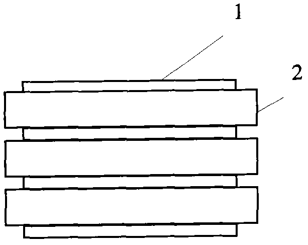
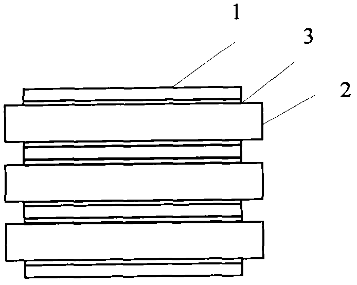
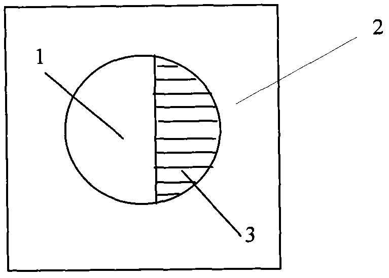
[0041] (2) Use DC magnetron sputtering coating technology to coat the two surfaces of the thin monolithic sheet obtained in step (1) into a dense nickel layer with a diameter of φ10mm as the interface transition layer electrode in the internal electrode, and then use screen printing technology on Ni The same area of ​​low-temperature silver paste electrode is coated on the surface of the film layer. According to the capacitance requirements, the glass-ceramic sheet printed with silver paste electrodes is subjected to multi-layer lamination treatment with micro-pressure, and sintered at 240°C to obtain a three-layer series internal electrode structure between multi-layer glass ceramic dielectric materials (schematic diagram as shown in Fig. Figure 4 shown).

[0042] (3) test leakage current, breakdown field ...

Embodiment 2

[0044] Glass-ceramic dielectric thin monolithic sample The thin monolithic acquisition method is the same as the step (1) of embodiment 1, adopting DC magnetron sputtering coating technology to be plated on the two surfaces of the thin monolithic obtained with a diameter of φ 10mm dense silver layer as the internal electrode The interfacial transition layer electrode, and then use screen printing technology to coat the same area of ​​low-temperature silver paste electrode on the surface of the Ag film layer. According to the capacitance requirements, the glass-ceramic sheet printed with silver paste electrodes is subjected to a multi-layer lamination process with micro-pressure, and sintered at 300 ° C to obtain a three-layer series internal electrode structure between multi-layer glass ceramic dielectric materials. And test the leakage current, the breakdown field strength, the dielectric constant of the capacitor of the gained glass-ceramic lamination (see respectively Figu...

Embodiment 3

[0047] Glass-ceramic dielectric thin monolithic sample The thin monolithic acquisition method is the same as the step (1) of embodiment 1, adopting DC magnetron sputtering coating technology to be plated on the two surfaces of the thin monolithic obtained with a diameter of φ10mm dense copper layer as the internal electrode The interfacial transition layer electrode, and then use screen printing technology to coat the same area of ​​low-temperature silver paste electrode on the surface of the Cu film layer. According to the capacitance requirements, the glass-ceramic sheet printed with silver paste electrodes is subjected to a multi-layer lamination process with micro-pressure, and sintered at 150 ° C to obtain a three-layer series internal electrode structure between multi-layer glass ceramic dielectric materials. And test the leakage current, the breakdown field strength, the dielectric constant of the capacitor of the gained glass-ceramic lamination (see respectively Figur...


PUM

PropertyMeasurementUnit
diameteraaaaaaaaaa
breakdown field strengthaaaaaaaaaa

Abstract

The invention discloses an inner electrode of a glass-ceramic stacked capacitor and a preparation method of the inner electrode in the technical field of functional materials. The inner electrode structurally comprises glass-ceramic dielectric layers and silver paste electrode layers which are stacked, wherein an inner electrode transition layer is arranged between one glass-ceramic dielectric layer and one silver paste electrode layer which are adjacent to each other. The preparation process of the inner electrode comprises the steps of: firstly plating a metal film on each of the two surfaces of each glass-ceramic dielectric single sheet to serve as the inner electrode transition layer; and then coating a low-temperature silver paste electrode on the surface of each of the plated metal film layers, stacking multiple layers and later, conducting sintering. According to the invention, the structure and the preparation method of the inner electrode which is used for the glass-ceramic stacked capacitor and can be sintered at low temperature are found out, so that the sintering temperature is lowered by over 300 DEG C, the self-owned electrical property of a glass-ceramic dielectric material is maintained, the dielectric constant is kept at 176 approximately and the direct-current breakdown field strength is increased to about 33kV/mm. The preparation method is very suitable for preparing the high-voltage-resistant inner electrode of the glass-ceramic stacked capacitor.

Description

technical field [0001] The invention belongs to the technical field of functional materials, and particularly relates to an internal electrode of a glass-ceramic laminated capacitor and a preparation method thereof, especially a high-strength electrode with lead niobate and sodium niobate as the ceramic phase and silicon dioxide as the glass phase. The invention discloses an internal electrode material for a multilayer capacitor based on a glass-ceramic material with high wear strength and high dielectric constant, and a preparation method thereof. Background technique [0002] Glass-ceramic materials have excellent ferroelectric and insulating properties due to their low-defect and void-free characteristics, and are widely used in small and large-capacity micro-multilayer ceramic capacitors, ultra-large-scale energy storage, and tuned microwave devices. One of the most widely used materials in ceramics. The internal electrode structure and material properties of the lamina...

Claims


Application Information

Patent Timeline
Patent Type & Authority Applications(China)
IPC IPC(8): H01G4/005H01G4/008H01G4/12H01G4/30
Inventor 杜军朱君罗君张庆猛唐群
Owner GENERAL RESEARCH INSTITUTE FOR NONFERROUS METALS BEIJNG
Why Eureka
Try Eureka