Process for preparing ultrathin gradient ZrGeN/CuGe composite barrier layer with high thermal stability
A preparation process and barrier layer technology, applied in the field of ultra-thin, high thermal stability ZrGeN/CuGe composite gradient barrier layer preparation process, to achieve low cost, reduce the thickness of the barrier layer, and reduce the effect of resistivity
- Summary
- Abstract
- Description
- Claims
- Application Information
AI Technical Summary
Problems solved by technology
Method used
Image
Examples
Embodiment 1
[0035] The preparation process of the ZrGeN / CuGe composite gradient barrier layer used in this embodiment includes the following steps:
[0036] a. Clean the substrate material:
[0037] After cleaning the single crystal silicon as the substrate material with hydrofluoric acid for 15 minutes, put it into acetone and absolute ethanol for 20 minutes of ultrasonic cleaning respectively, put it into a vacuum chamber after drying, and then evacuate to a degree of 2.0×10 -4 Pa;
[0038] b. Treatment of the substrate before deposition:
[0039] Keep the background vacuum of the vacuum chamber at 2.0×10 -4 Under Pa, clean with bias backsputter for 10 minutes and pre-sputter for 5 minutes to remove Si substrate and target impurities; backsputter power is 150 W; pre-sputter power is 150 W; backsputter bias and pre-sputter bias The pressures are -500 V and -150 V respectively; the back-splash and pre-splash gases are both Ar; the working vacuum is 2.0 Pa;
[0040] c. Deposition of ...
Embodiment 2
[0049] The operation steps of this embodiment, the coating equipment used and other working conditions are all the same as in Example 1, and the deposition thickness of the double-layer gradient diffusion barrier layer is kept constant at 15 nm, and the deposition time of the ZrGeN layer, the ZrGeN gradient layer and the CuGe layer is adjusted. , so as to change the thickness of the ZrGeN layer, the ZrGeN gradient layer and the CuGe layer in the double-layer gradient diffusion barrier layer, and also meet its ultra-thin and high thermal stability performance.
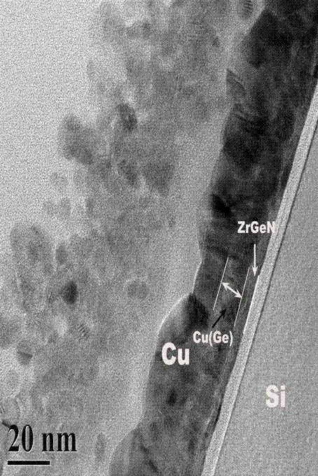
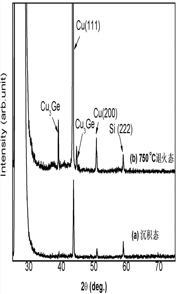
[0050] In this example, the deposition time of the ZrGeN layer is 20 s, and the deposition thickness is 3 nm; the deposition time of the ZrGeN gradient layer is 40 s, and the deposition thickness is 5 nm; the deposition time of the CuGe layer is 21 s, and the deposition thickness is 7 nm. ZrGeN (8 nm) / CuGe (7 nm) composite graded barrier layer sample. The obtained samples were annealed in vacuum at 750°C for 40 min an...
Embodiment 3
[0052] The operation steps of this embodiment, the coating equipment used and other working conditions are all the same as in Example 1, and the deposition thickness of the double-layer gradient diffusion barrier layer is kept constant at 15 nm, and the deposition time of the ZrGeN layer, the ZrGeN gradient layer and the CuGe layer is adjusted. , so as to change the thickness of the ZrGeN layer, the ZrGeN gradient layer and the CuGe layer in the double-layer gradient diffusion barrier layer, and also meet its ultra-thin and high thermal stability performance.
[0053] In this example, the deposition time of the ZrGeN layer is 8 s, and the deposition thickness is 1 nm; the deposition time of the ZrGeN gradient layer is 32 s, and the deposition thickness is 4 nm; the deposition time of the CuGe layer is 30 s, and the deposition thickness is 10 nm. ZrGeN (5 nm) / CuGe (10 nm) composite graded barrier layer samples. The obtained samples were tested by XRD after vacuum annealing at...
PUM
| Property | Measurement | Unit |
|---|---|---|
| thickness | aaaaa | aaaaa |
| thickness | aaaaa | aaaaa |
| electrical resistivity | aaaaa | aaaaa |
Abstract
Description
Claims
Application Information


