MEMS (micro-electromechanical system) and IC (integrated circuit) monolithical integration method

A monolithic integration, substrate technology, applied in coatings, microstructure devices, microstructure technology, etc., can solve the problems of low stress, difficult to make silicon nitride films, etc., achieve high yield and simplify integration Manufacturing process, the effect of reducing parasitic capacitance and distributed capacitance

Inactive Publication Date: 2014-11-26
PEKING UNIV
View PDF4 Cites 0 Cited by
  • Summary
  • Abstract
  • Description
  • Claims
  • Application Information

AI Technical Summary

Problems solved by technology

At present, some of the integration solutions of well-known chip companies such as ADI use PECVD silicon nitride, and some use LPCVD low-stress silicon nitride. These solutions have high controllability for processing equipment and processes. requirements, the silicon nitride film that needs to be produced has both low stress and high corrosion selection ratio, and it is difficult for general equipment to make a silicon nitride film that meets the demand

Method used


Image

  • MEMS (micro-electromechanical system) and IC (integrated circuit) monolithical integration method
  • MEMS (micro-electromechanical system) and IC (integrated circuit) monolithical integration method
  • MEMS (micro-electromechanical system) and IC (integrated circuit) monolithical integration method

Examples


Embodiment 1

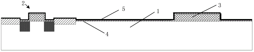
[0039] The method of the present invention is specifically described below by taking the preparation of a monolithic integrated flat capacitive resonator as an example, and the manufacturing steps are as follows:

[0040] 1. The monocrystalline silicon substrate is used as the substrate 1 of the chip, and the CMOS circuit 2 is manufactured on the substrate 1 by IC technology, and all processes except metal interconnection are completed; MEMS devices can be manufactured at the same time when the polysilicon gate of the MOS device is manufactured polysilicon bottom electrode 3

[0041] 2. Deposit IC area protection layer, including: LPCVD silicon oxide 3000 LPCVD silicon nitride 1800 Form a silicon oxide layer 4 and a silicon nitride layer 5 on the entire substrate 1, as shown in Figure 1(a);

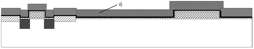
[0042] 3. Use MEMS surface sacrificial layer technology to make movable structures, including:

[0043] a) LPCVD phosphosilicate glass with a thickness of 1 μm, forming a phosphosili...


PUM


Abstract

The invention discloses an MEMS and IC monolithical integration method. The method comprises the following steps: 1, completing all IC technologies except a metal interconnection technology on a substrate, and sequentially depositing a silicon oxide layer and a silicon nitride layer which are used as protection layers of an IC region; 2, making an MEMS structure through adopting an MEMS surface sacrificial layer technology; 3, etching to remove the silicon nitride protection layer of the IC region, etching the silicon oxide protection layer to form a lead hole, depositing and imaging the metal to form the metal interconnection; and 4, removing the sacrificial layer of an MEMS region, and releasing the MEMS movable structure. The method needs no special low-stress silicon nitride production equipment, adopts above IC-MEMS intersection technology, and allows the internal stress of integrated chips to be controlled through selectively removing the silicon nitride protection layer, so the influence of the integration technology to the IC performances is reduced, and the technology is simple and reliable.

Description

technical field [0001] The invention belongs to the field of micro-electro-mechanical systems (MEMS) and integrated circuit IC (CMOS) processing technology, and relates to a monolithic integration method of MEMS and IC technology, and adopts a mixed technology method of MEMS-IC-MEMS to simultaneously form MEMS and IC on a single wafer. The CMOS part is especially used in the field of manufacturing MEMS chips containing CMOS circuits. Background technique [0002] There are many advantages of monolithic integration of MEMS and IC, including reducing parasitic capacitance, reducing chip size, reducing cost, reducing packaging pressure, and improving reliability. The usually selected integration scheme is made by MEMS process after IC, that is, post-CMOS process. The design of post-CMOS integration scheme focuses on how to control the influence of MEMS process on IC circuit. Since IC circuits are composed of single-transistor NMOS or PMOS, studies have shown that the performa...

Claims


Application Information

Patent Timeline
Patent Type & Authority Patents(China)
IPC IPC(8): B81C1/00
Inventor 赵丹淇张大成林琛何军杨芳田大宇刘鹏王玮李婷罗葵
Owner PEKING UNIV
Why Eureka
Try Eureka