LED (Light Emitting Diode) surface patterning method

A surface pattern and surface material technology, applied in the direction of electrical components, circuits, semiconductor devices, etc., can solve the problems of reducing light extraction efficiency and achieve the effect of simple preparation principle, low cost and high yield

Inactive Publication Date: 2012-07-18
SUN YAT SEN UNIV
View PDF4 Cites 13 Cited by
  • Summary
  • Abstract
  • Description
  • Claims
  • Application Information

AI Technical Summary

Problems solved by technology

Since the light generated by the multi-quantum well layer is limited by total internal reflection during the exit process, only the light within the light cone (about 23°) can exit, which greatly reduces the light extraction efficiency of the LED.

Method used


Image

  • LED (Light Emitting Diode) surface patterning method
  • LED (Light Emitting Diode) surface patterning method
  • LED (Light Emitting Diode) surface patterning method

Examples


Embodiment 1

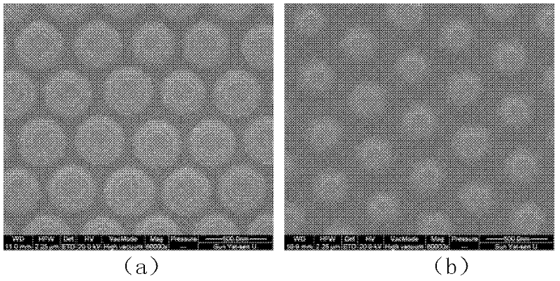
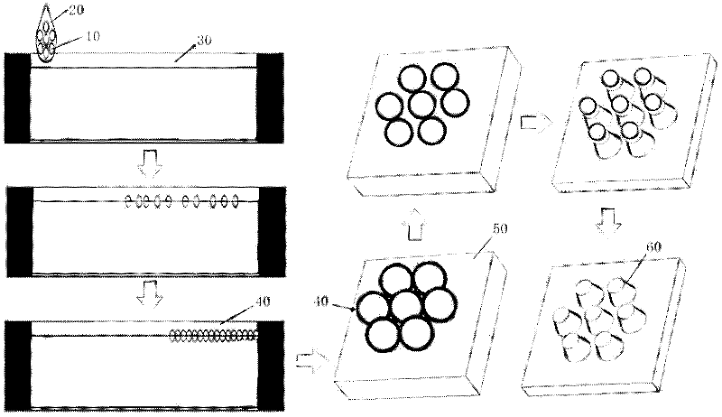
[0047] Take the polystyrene microsphere solution with a diameter of 450nm and mix it with alcohol in equal proportions, and then transfer the polystyrene microspheres to the surface of deionized water with a small-bore syringe and slide buffer to spread evenly. Dropping sodium lauryl sulfate active agent changes the surface tension of water, making the microspheres aggregate and self-assemble into a hexagonal close-packed array to form a polystyrene monolayer microsphere film, such as figure 2 (a) shown. Transfer the single-layer microsphere film to the surface of the LED, and heat the LED at 70°C for 20 minutes, so that each microsphere in the single-layer microsphere film adheres to the surface of the LED to avoid drifting and damage of the microspheres. lattice array. Then clean the sample with oxygen ions, the experimental power is 35W, the oxygen flow rate is 600sccm, and the cleaning time is about 180s.

[0048] Then etch the single-layer microsphere film 9s and 15s i...

Embodiment 2

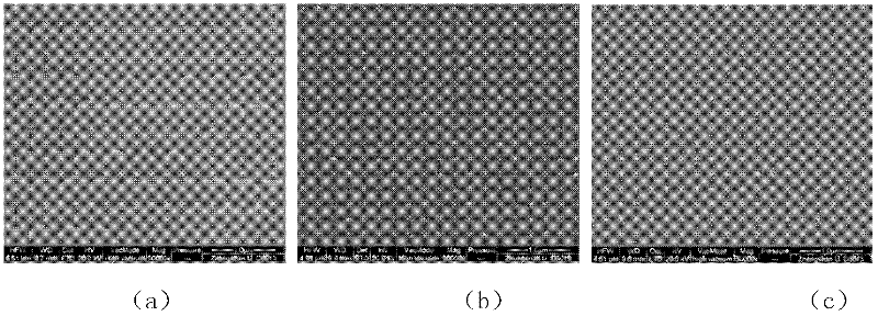
[0050] Take the polystyrene microsphere solution with a diameter of 308nm and mix it with alcohol in equal proportions, then transfer the polystyrene microspheres to the surface of deionized water and spread them evenly using a small-bore syringe and slide buffer. Dropping sodium lauryl sulfate active agent changes the surface tension of water, making the microspheres aggregate and self-assemble into a hexagonal close-packed array to form a polystyrene monolayer microsphere film, such as figure 2 (b) shown. Transfer the single-layer microsphere film to the surface of the LED, and heat the LED at 70°C for 20 minutes, so that each microsphere in the single-layer microsphere film adheres to the surface of the LED to avoid drifting and damage of the microspheres. lattice array. Then clean the sample with oxygen ions, the experimental power is 35W, the oxygen flow rate is 600sccm, and the cleaning time is about 180s.

[0051] Then etch the single-layer microsphere film 11s in th...

Embodiment 3

[0053] Take the polystyrene microsphere solution with a diameter of 187nm and mix it with alcohol in equal proportions, then transfer the polystyrene microspheres to the surface of deionized water with a small-bore syringe and slide buffer to spread evenly. Dropping sodium lauryl sulfate active agent changes the surface tension of water, making the microspheres aggregate and self-assemble into a hexagonal close-packed array to form a polystyrene monolayer microsphere film, such as figure 2 (c) shown. Transfer the single-layer microsphere film to the surface of the LED, and heat the LED at 70°C for 20 minutes, so that each microsphere in the single-layer microsphere film adheres to the surface of the LED to avoid drifting and damage of the microspheres. lattice array. Then clean the sample with oxygen ions, the experimental power is 35W, the oxygen flow rate is 600sccm, and the cleaning time is about 60s.

[0054] Then etch the single-layer microsphere film in the vertical d...


PUM


Abstract

The invention discloses an LED (Light Emitting Diode) surface patterning method. The method comprises the following steps of: mixing a monodispersed microsphere solution and alcohol; and then transferring the monodispersed microsphere to the surface of deionized water by a buffer; uniformly dispersing the monodispersed microsphere and the deionized water; dripping a surfactant to the mixture so as to change the surface tension of the water so that microspheres are intensively arranged in a hexagonal shape in a self-assembled way to form a single-layer microsphere film; transferring the single-layer microsphere film to an LED surface; heating a sample; using a microsphere fixing position as an etching mask to etch an LED surface material; peeling off the rest mask material; and obtaining a nanometer truncated cone array as an LED surface roughened pattern so that the LED light extracting efficiency can be obviously increased. The period, duty cycle and truncated cone unit shape of the truncated cone array pattern can be controlled by changing microsphere diameter, etching power, oxygen flow and etching time; and the LED surface patterning method disclosed by the invention has the advantages of simple design principle, low preparation cost and easiness in operation.

Description

technical field [0001] The invention relates to an LED, in particular to a novel LED surface patterning method. Background technique [0002] Semiconductor solid-state light source LED is known as the best choice for next-generation light source because of its energy saving, long service life, and environmental friendliness. There are two main parameters to characterize LED luminous efficiency: internal quantum efficiency and extraction efficiency. In recent years, with the improvement of chip epitaxial growth technology (for example: epitaxial lateral overgrowth), the internal quantum efficiency of LED has reached more than 80%. In contrast, there is still a lot of room for improvement in LED light extraction efficiency. Since the light generated by the multi-quantum well layer is limited by total internal reflection during the exit process, only the light within the light cone (about 23°) can exit, which greatly reduces the light extraction efficiency of the LED. For a ...

Claims


Application Information

Patent Timeline
Patent Type & Authority Applications(China)
IPC IPC(8): H01L33/00H01L33/22
Inventor 金崇君梁柱洪
Owner SUN YAT SEN UNIV
Why Eureka
Try Eureka